
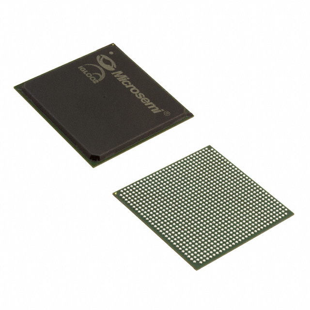
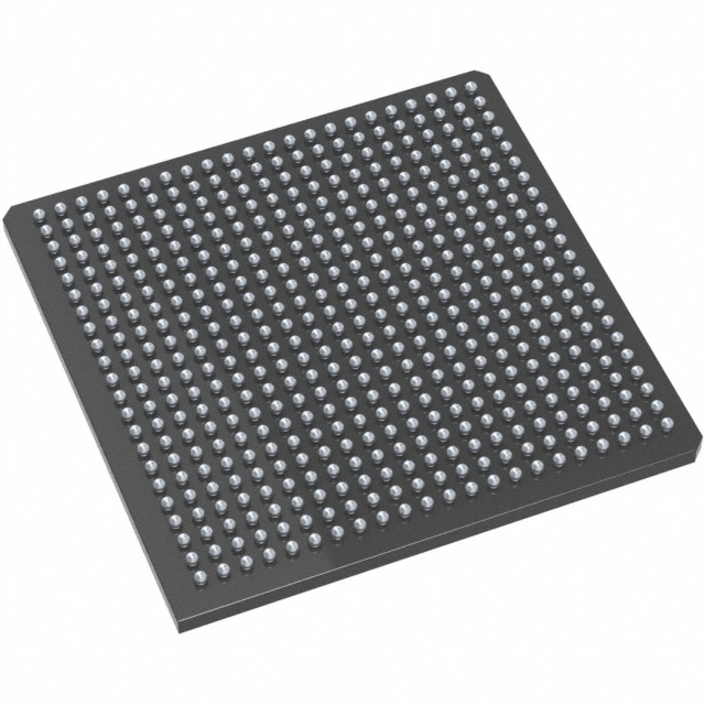
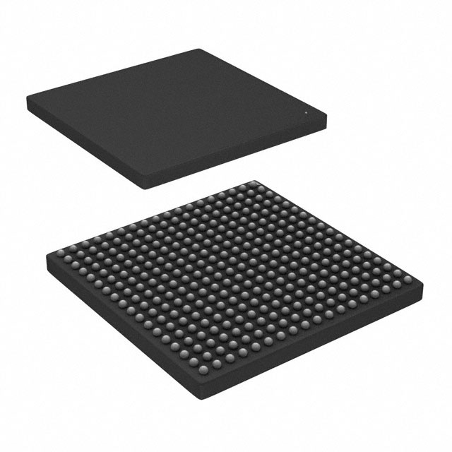
M2GL050T-FG896
| Part Description |
IGLOO2 Field Programmable Gate Array (FPGA) IC 377 1869824 56340 896-BGA |
|---|---|
| Quantity | 797 Available (as of June 15, 2026) |
| Product Category | Field Programmable Gate Array (FPGA) |
|---|---|
| Manufacturer | Microchip Technology |
| Manufacturing Status | Active |
| Manufacturer Standard Lead Time | 16 Weeks |
| Datasheet |
Specifications & Environmental
| Device Package | 896-FBGA (31x31) | Grade | Commercial | Operating Temperature | 0°C – 85°C | ||
|---|---|---|---|---|---|---|---|
| Package / Case | 896-BGA | Number of I/O | 377 | Voltage | 1.14 V - 2.625 V | ||
| Mounting Method | Surface Mount | RoHS Compliance | RoHS non-compliant | REACH Compliance | REACH Unaffected | ||
| Moisture Sensitivity Level | 3 (168 Hours) | Number of LABs/CLBs | 56340 | Number of Logic Elements/Cells | 56340 | ||
| Number of Gates | N/A | ECCN | 3A991D | HTS Code | 8542.39.0001 | ||
| Qualification | N/A | Total RAM Bits | 1869824 |
Overview of M2GL050T-FG896 – IGLOO2 Field Programmable Gate Array (FPGA) IC, 377 I/Os, 896-BGA
The M2GL050T-FG896 is a Microchip Technology IGLOO2 flash-based FPGA optimized for applications requiring high integration, security features, and efficient logic fabric. Built on the IGLOO2 architecture, it combines a fourth-generation flash FPGA fabric with high-performance communications and memory interfaces to address embedded, communications, and DSP-focused designs.
With 56,340 logic elements, extensive embedded memory resources, multi-standard I/O support and on-chip system IP from the IGLOO2 family, this device targets designers needing scalable programmable logic with commercial-grade operating conditions and RoHS compliance.
Key Features
- Logic Fabric — 56,340 logic elements implemented with efficient 4-input LUTs and carry chains for compact logic and arithmetic implementations.
- Embedded Memory — Approximately 1.87 Mbits of total on-chip RAM capacity, complemented by IGLOO2 family memory architecture that includes eSRAM and embedded nonvolatile memory options.
- DSP and Math Resources — IGLOO2 family mathblocks and DSP-capable resources for signed/unsigned multiplication and accumulation suited to signal processing tasks.
- High-Speed Serial Interfaces — Series-level support for up to 16 SERDES lanes, PCI Express endpoints and XAUI/XGXS interfaces to enable high-bandwidth serial communications.
- DDR Memory Controllers — Integrated DDRx memory controller support (DDR2/DDR3/LPDDR options at the series level) for high-speed external memory interfacing.
- I/O and Voltage — 377 user I/Os with multi-standard I/O support and a supply voltage range of 1.14 V to 2.625 V to accommodate diverse signaling standards.
- Package and Mounting — 896-ball FBGA package (31 × 31 mm) designed for surface-mount assembly.
- Operating Range and Compliance — Commercial-grade operating temperature from 0 °C to 85 °C and RoHS compliant.
- Security and Reliability (Series Capabilities) — IGLOO2 family security features such as encrypted bitstream loading, device certificates and anti-tamper options to protect IP and supply-chain integrity.
Typical Applications
- High-Speed Networking and Connectivity — Implement backplane, switch or PHY interface logic using SERDES lanes and PCIe support for high-throughput links.
- Memory-Intensive Embedded Systems — Use on-chip RAM and DDRx memory controllers for buffering, packet processing or frame storage in embedded controllers and appliances.
- Digital Signal Processing — Leverage mathblocks and DSP resources for filtering, decoding and other real-time signal processing tasks.
- Secure Programmable Logic — Protect firmware and IP in applications requiring encrypted bitstreams and device-level security features.
Unique Advantages
- High Logic Density: 56,340 logic elements provide substantial routing and logic capacity for mid-range FPGA designs without external logic proliferation.
- Integrated Memory Resources: Approximately 1.87 Mbits of embedded RAM plus on-chip nonvolatile options reduce external memory requirements and simplify board design.
- Versatile High-Speed I/O: 377 multi-standard I/Os and series support for SERDES and PCIe enable flexible interfacing to modern peripherals and networks.
- Commercial-Grade Reliability: Rated for 0 °C to 85 °C and RoHS compliant for mainstream electronics applications.
- Compact, Surface-Mount Package: 896-FBGA (31×31 mm) delivers high pin count in a space-efficient package suitable for dense PCB layouts.
- Design Security Features: Series-level encrypted bitstream loading and supply-chain device certificates help secure IP and device provisioning.
Why Choose M2GL050T-FG896?
The M2GL050T-FG896 delivers a balance of logic capacity, embedded memory, and high-speed I/O in a single, flash-based FPGA package. Its IGLOO2 architecture provides DSP resources, serial communications capabilities and on-chip memory structures that help reduce BOM complexity and accelerate time to market for embedded and communications designs.
This device is well suited to customers designing commercial-grade systems that require substantial logic resources, multi-standard interfacing and integrated security options, while maintaining a compact 896-FBGA footprint and broad voltage support.
Request a quote or submit an inquiry for pricing and availability of the M2GL050T-FG896 to begin integrating this IGLOO2 FPGA into your next design.


Date Founded: 1989
Headquarters: Chandler, Arizona, USA
Employees: 22,000+
Revenue: $8.349 Billion
Certifications and Memberships: ISO9001:2015, IATF16949:2016, AS 9100D


