
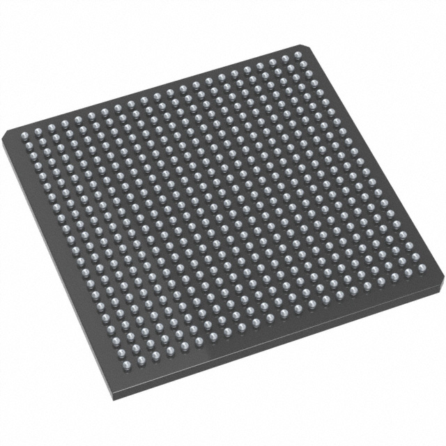
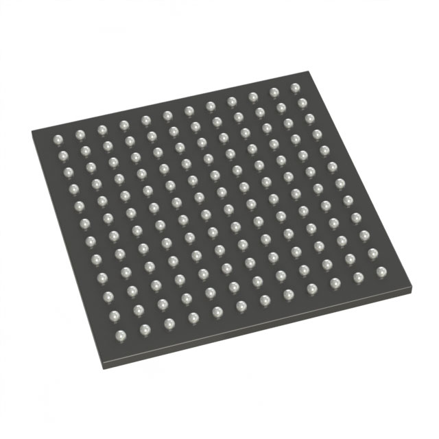
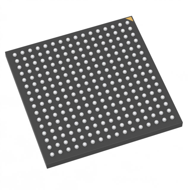
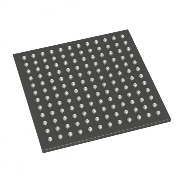
M7A3P1000-FG484
| Part Description |
ProASIC3 Field Programmable Gate Array (FPGA) IC 300 147456 484-BGA |
|---|---|
| Quantity | 1,041 Available (as of October 7, 2026) |
| Product Category | Field Programmable Gate Array (FPGA) |
|---|---|
| Manufacturer | Microchip Technology |
| Manufacturing Status | Active |
| Manufacturer Standard Lead Time | 12 Weeks |
| Datasheet |
Specifications & Environmental
| Device Package | 484-FPBGA (23x23) | Grade | Commercial | Operating Temperature | 0°C – 85°C | ||
|---|---|---|---|---|---|---|---|
| Package / Case | 484-BGA | Number of I/O | 300 | Voltage | 1.425 V - 1.575 V | ||
| Mounting Method | Surface Mount | RoHS Compliance | RoHS non-compliant | REACH Compliance | REACH Unaffected | ||
| Moisture Sensitivity Level | 3 (168 Hours) | Number of LABs/CLBs | 24576 | Number of Logic Elements/Cells | 24576 | ||
| Number of Gates | 1000000 | ECCN | 3A991D | HTS Code | 8542.39.0001 | ||
| Qualification | N/A | Total RAM Bits | 147456 |
Overview of M7A3P1000-FG484 – ProASIC3 Field Programmable Gate Array (FPGA) IC 300 147456 484-BGA
The M7A3P1000-FG484 is a ProASIC3 family field programmable gate array (FPGA) from Microchip Technology targeted at commercial applications. It provides a balance of logic capacity, on-chip memory, and I/O density for custom digital designs implemented on a surface-mount 484-BGA package.
Designed for use in commercial electronic systems, the device supports designs requiring up to 24,576 logic elements, approximately 147,456 bits of embedded memory, and up to 300 I/O pins while operating within a 1.425 V to 1.575 V supply range and a 0 °C to 85 °C temperature window.
Key Features
- Core Capacity 24,576 logic elements and a reported 1,000,000 equivalent gates provide the programmable resources for complex digital functions and custom logic implementations.
- On-Chip Memory Approximately 147,456 bits (≈0.147 Mbits) of embedded RAM for buffering, state storage, and small data structures within the FPGA fabric.
- I/O Density Up to 300 user I/O pins to support parallel interfaces, bus connections, and multiple peripheral signals in compact systems.
- Power and Supply Operates from a supply range of 1.425 V to 1.575 V, enabling integration into designs with tightly specified core voltage rails.
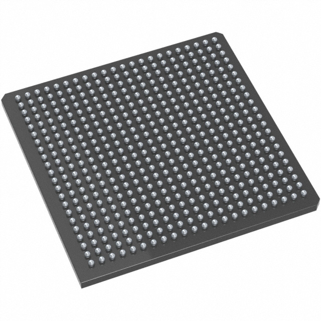
- Package and Mounting 484-ball BGA package (supplier device package: 484-FPBGA (23×23)), optimized for surface-mount PCB assembly to save board area while delivering high pin count.
- Operating Range Commercial-grade temperature range from 0 °C to 85 °C for general-purpose electronics and OEM products.
- Standards Compliance RoHS compliant, meeting lead-free and hazardous substance requirements for commercial electronics manufacturing.
Typical Applications
- Commercial Electronics — Implement custom control logic, peripheral interfaces, and glue-logic in consumer and enterprise equipment using the device's logic and I/O resources.
- Connectivity and Interface Modules — Handle bus bridging, protocol translation, and parallel interface aggregation where substantial I/O and custom logic are required.
- Embedded Subsystems — Provide configurable compute and buffering functions for OEM subsystems that need on-chip RAM and flexible logic resources.
- Prototyping and Product Development — Suitable for developing and validating digital architectures that fit within the device’s logic and memory budgets before production deployment.
Unique Advantages
- High Logic Density: 24,576 logic elements allow implementation of sizeable custom logic blocks without external CPLDs or discrete logic.
- Substantial On-Chip Memory: Approximately 147,456 bits of embedded RAM reduce the need for external memory in moderate buffering and state-storage tasks.
- Large I/O Count: 300 I/O pins support complex system interconnects and multiple peripheral interfaces from a single device.
- Compact BGA Footprint: 484-FPBGA (23×23) simplifies high-density PCB layouts while delivering a high pin count in a surface-mount package.
- Commercial Temperature and RoHS Compliance: Rated for 0 °C to 85 °C operation and RoHS compliant for broad commercial deployment and regulatory alignment.
- Clear Power Specification: Narrow core supply range (1.425 V to 1.575 V) supports consistent power design and voltage regulation strategies.
Why Choose M7A3P1000-FG484?
The M7A3P1000-FG484 positions itself as a commercially focused, mid-to-high density FPGA option from Microchip Technology, combining a significant logic element count, on-chip RAM, and a high I/O complement in a compact 484-BGA package. These characteristics make it well suited to designers building commercial embedded systems, interface concentrators, and OEM modules that require programmable logic without excessive board area or external component count.
Backed by Microchip Technology, the part provides a predictable feature set for projects that demand a clear balance of integration, I/O capability, and memory resources. For teams targeting commercial-grade products where these specific capacities match the design requirements, the M7A3P1000-FG484 offers a reliable platform to implement and scale digital logic functions.
Request a quote or submit an inquiry to receive pricing, lead-time, and availability information for the M7A3P1000-FG484.





















Date Founded: 1989
Headquarters: Chandler, Arizona, USA
Employees: 22,000+
Revenue: $8.349 Billion
Certifications and Memberships: ISO9001:2015, IATF16949:2016, AS 9100D




