
M7AFS600-1FG256
| Part Description |
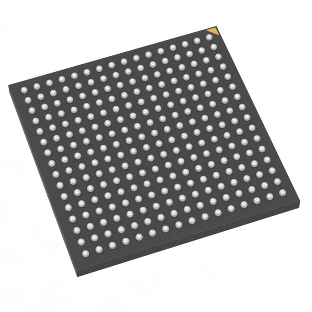
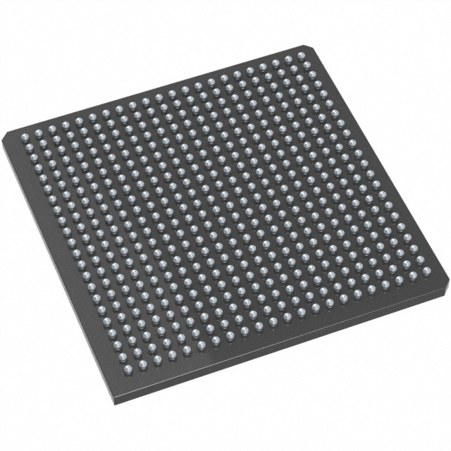
Fusion® Field Programmable Gate Array (FPGA) IC 119 110592 256-LBGA |
|---|---|
| Quantity | 998 Available (as of June 18, 2026) |
| Product Category | Field Programmable Gate Array (FPGA) |
|---|---|
| Manufacturer | Microchip Technology |
| Manufacturing Status | Active |
| Manufacturer Standard Lead Time | 16 Weeks |
| Datasheet |
Specifications & Environmental
| Device Package | 256-FPBGA (17x17) | Grade | Commercial | Operating Temperature | 0°C – 70°C | ||
|---|---|---|---|---|---|---|---|
| Package / Case | 256-LBGA | Number of I/O | 119 | Voltage | 1.425 V - 1.575 V | ||
| Mounting Method | Surface Mount | RoHS Compliance | RoHS non-compliant | REACH Compliance | REACH Unaffected | ||
| Moisture Sensitivity Level | 3 (168 Hours) | Number of LABs/CLBs | 13824 | Number of Logic Elements/Cells | 13824 | ||
| Number of Gates | 600000 | ECCN | 3A991D | HTS Code | 8542.39.0001 | ||
| Qualification | N/A | Total RAM Bits | 110592 |
Overview of M7AFS600-1FG256 – Fusion® Field Programmable Gate Array (FPGA) IC 119 110592 256-LBGA
The M7AFS600-1FG256 is a Fusion family mixed-signal, flash-based FPGA from Microchip Technology. It combines reprogrammable digital fabric with integrated analog peripherals and MOSFET gate-driver capability to address mixed-signal embedded designs.
Designed for applications that require on-chip analog integration and nonvolatile configuration, the device delivers up to 600,000 system gates, 13,824 logic elements, and embedded memory resources while operating in a compact 256‑LBGA package.
Key Features
- Core Logic and Capacity — Approximately 600,000 system gates and 13,824 logic elements provide the programmable logic resources required for complex control and signal-processing functions.
- Embedded Memory — Approximately 110,592 bits of on-chip RAM (about 108 kbits) for FIFOs and working storage, and Fusion-family embedded flash memory blocks as specified in the Fusion datasheet.
- Mixed-Signal Integration — Integrated A/D converter support up to 12-bit resolution and up to 600 ksps, with up to 30 analog input channels and on-chip temperature/current monitoring blocks.
- MOSFET Gate Drivers — Up to 10 gate-driver outputs with programmable drive strengths and support for P- and N-channel MOSFETs for power conversion and motor-drive interfaces.
- I/O Flexibility — 119 I/Os in the 256‑LBGA package with bank-selectable I/O voltages and support for single-ended and differential standards (LVTTL, LVCMOS, LVPECL, LVDS, B-LVDS, M-LVDS) as described in the Fusion family data.
- Clocking and Timing — On-chip clock support including an internal 100 MHz RC oscillator, crystal oscillator support, six Clock Conditioning Circuits (CCCs) and integrated PLL capability for clock conditioning and synthesis.
- Power and Supply — Core supply range 1.425 V to 1.575 V; Fusion-family devices support a single 3.3 V power supply with an on-chip 1.5 V regulator per the datasheet.
- Security and In-System Programming — ISP capabilities with AES-based security and FlashLock protection as implemented in the Fusion family for secure field updates.
- Package and Operating Range — Surface-mount 256‑LBGA (256‑FPBGA, 17×17) package; commercial-grade operating temperature 0 °C to 70 °C; RoHS compliant.
Typical Applications
- Power conversion and motor control — Integrated MOSFET gate-driver outputs and ADC channels simplify closed-loop power and motor-drive control implementations.
- Mixed-signal sensor interfaces — On-chip 12-bit ADC and multiple analog input channels enable direct connection and preprocessing of analog sensors and monitors.
- Embedded control and logic consolidation — Use programmable logic and embedded memory to consolidate glue logic, protocol bridging, and control functions into a single device.
- Compact systems with space constraints — 256‑LBGA package and integrated analog peripherals reduce external component count for space- and BOM-sensitive designs.
Unique Advantages
- Highly integrated mixed-signal platform: Combines programmable logic, ADCs, and MOSFET gate drivers to reduce external components and simplify board design.
- Nonvolatile, instant-on configuration: Flash-based architecture preserves configuration without external memory and enables immediate startup behaviors.
- Flexible I/O and voltage support: Bank-selectable I/O voltages and broad I/O standard support enable interfacing with a wide range of peripherals and sensors.
- Secure in-system updates: ISP with AES-based protection and FlashLock help safeguard firmware and configuration in the field.
- Compact package with ample I/O: 119 I/Os in a 256‑LBGA package provide a balance of connectivity and board-level density for embedded applications.
Why Choose M7AFS600-1FG256?
The M7AFS600-1FG256 positions itself as a mixed-signal FPGA option for designs that require substantial programmable logic (approximately 13,824 logic elements / ~600k gates) together with integrated analog functionality and MOSFET gate-driving capability. Its Fusion family architecture delivers nonvolatile, flash-based configuration with on-chip analog and clocking resources to simplify system design and speed development.
This device is suited to embedded systems engineers and procurement teams seeking a single-chip solution to consolidate control, sensing, and power-drive functions in commercial-temperature applications while benefiting from Microchip Technology's Fusion family feature set and RoHS compliance.
Request a quote or submit an inquiry for pricing, availability, and lead-time information on the M7AFS600-1FG256.


Date Founded: 1989
Headquarters: Chandler, Arizona, USA
Employees: 22,000+
Revenue: $8.349 Billion
Certifications and Memberships: ISO9001:2015, IATF16949:2016, AS 9100D


