
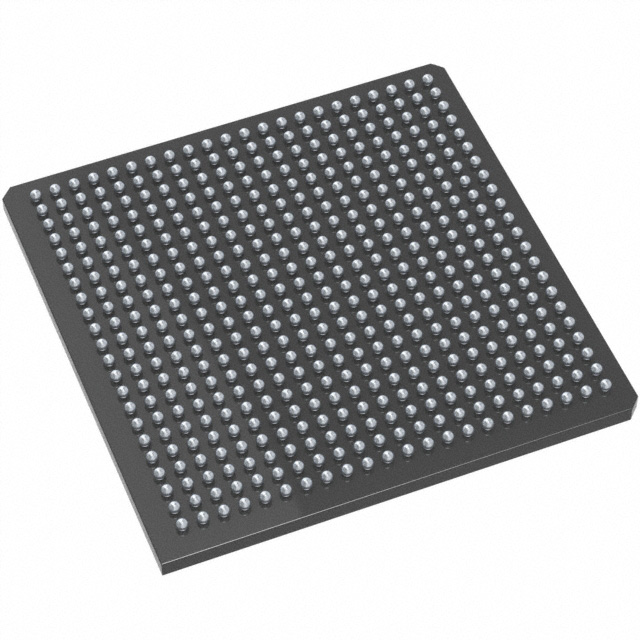
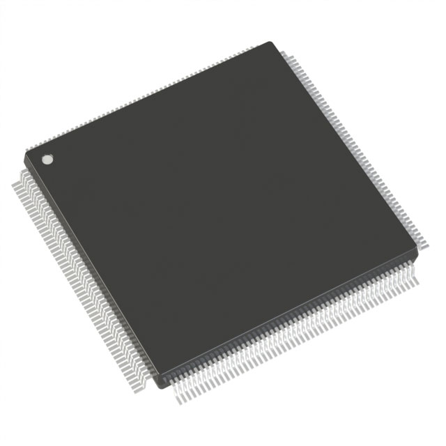
M7AFS600-1FG484I
| Part Description |
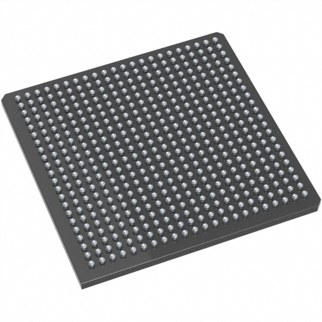
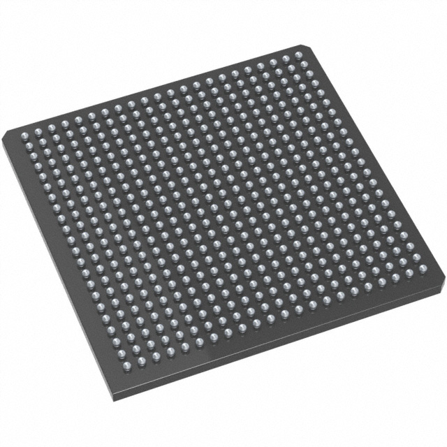
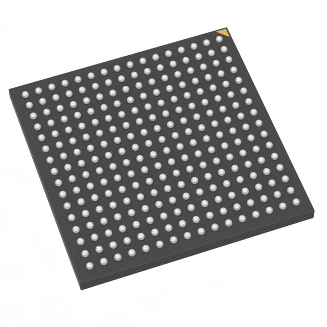
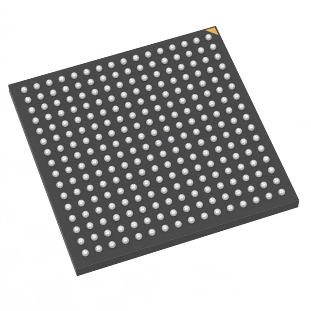
Fusion® Field Programmable Gate Array (FPGA) IC 172 110592 484-BGA |
|---|---|
| Quantity | 317 Available (as of October 8, 2026) |
| Product Category | Field Programmable Gate Array (FPGA) |
|---|---|
| Manufacturer | Microchip Technology |
| Manufacturing Status | Active |
| Manufacturer Standard Lead Time | 16 Weeks |
| Datasheet |
Specifications & Environmental
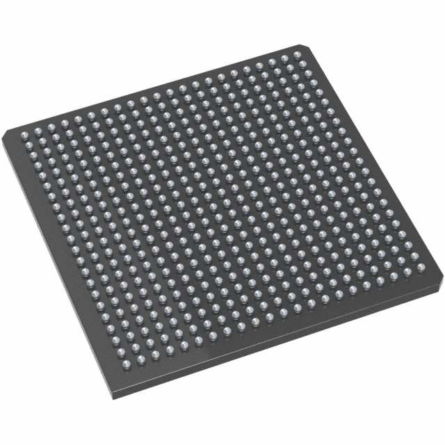
| Device Package | 484-FPBGA (23x23) | Grade | Industrial | Operating Temperature | -40°C – 85°C | ||
|---|---|---|---|---|---|---|---|
| Package / Case | 484-BGA | Number of I/O | 172 | Voltage | 1.425 V - 1.575 V | ||
| Mounting Method | Surface Mount | RoHS Compliance | RoHS non-compliant | REACH Compliance | REACH Unaffected | ||
| Moisture Sensitivity Level | 3 (168 Hours) | Number of LABs/CLBs | 13824 | Number of Logic Elements/Cells | 13824 | ||
| Number of Gates | 600000 | ECCN | 3A991D | HTS Code | 8542.39.0001 | ||
| Qualification | N/A | Total RAM Bits | 110592 |
Overview of M7AFS600-1FG484I – Fusion® Field Programmable Gate Array (FPGA) IC 172 110592 484-BGA
The M7AFS600-1FG484I is a Fusion® family mixed-signal FPGA from Microchip Technology, offering a flash-based, nonvolatile architecture optimized for industrial embedded applications. It integrates digital logic, embedded memory, precision analog resources and MOSFET gate-driver capability in a 484-BGA package, enabling compact, instant-on system designs.
Designed for mixed-signal control and instrumentation, the device combines 600,000 logic gates (13,824 logic elements), 110,592 bits of on-chip RAM, and embedded flash memory, along with analog front-end and clocking resources to address sensor interfacing, power control and general-purpose I/O-centric applications in industrial environments.
Key Features
- Core and Logic 600,000 system gates and 13,824 logic elements (tiles) provide substantial programmable logic capacity for control and glue-logic tasks.
- Embedded RAM 110,592 bits of on-chip RAM (~108 kbits) for FIFOs, buffering and scratch memory.
- Embedded Flash Memory Fusion AFS600 family devices include 4 Mbits of on-chip flash for nonvolatile configuration and user storage.
- Analog and Mixed-Signal Integrated ADC capability (up to 12-bit resolution and up to 600 ksps) with up to 30 analog input channels and analog quads for sensor and signal-conditioning integration.
- MOSFET Gate Drivers Up to 10 MOSFET gate-driver outputs with programmable drive strengths and support for P- and N-channel devices, enabling direct power-stage interfacing.
- I/O and Bank Options 172 digital I/Os in the 484-BGA package with support for mixed-voltage operation and multiple I/O standards (bank-selectable voltages across the Fusion family).
- Clocking Family-level clocking delivers up to 350 MHz system performance with Clock Conditioning Circuits (CCCs) and two integrated PLLs for phase shift, multiply/divide and frequency conditioning.
- Security and In-System Programming ISP with 128-bit AES via JTAG and FlashLock® support to protect configuration and enable secure field updates.
- Power and Voltage Documented core supply range: 1.425 V to 1.575 V. Fusion family devices support a single 3.3 V power supply with an on-chip 1.5 V regulator and include low-power modes (sleep/standby).
- Package and Environmental Surface-mount 484-FPBGA (23×23) package, industrial temperature grade with operating range −40 °C to 85 °C, and RoHS compliant.
Typical Applications
- Industrial Motor and Power Control On-chip MOSFET gate drivers and integrated ADCs support direct interfacing to power stages and closed-loop motor control schemes.
- Sensor Aggregation and Signal Conditioning Multiple analog input channels with precision ADC capability enable consolidation of sensor inputs and preprocessing within a single IC.
- Embedded Control and Instrumentation Programmable logic, embedded flash and on-chip RAM provide a compact platform for control logic, sequencing and data buffering in industrial instruments.
- Mixed-Voltage I/O Systems Bank-selectable I/O voltages and a wide set of digital standards allow integration across multiple logic domains and peripheral interfaces.
Unique Advantages
- Highly integrated mixed-signal platform: Combines logic, embedded flash, RAM and analog front-end to reduce BOM and simplify board-level design.
- Nonvolatile, instant-on operation: Flash-based configuration eliminates external configuration memory and delivers immediate startup behavior.
- Industrial-grade operation: Specified for −40 °C to 85 °C and supplied in a 484-BGA surface-mount package suited to industrial applications.
- Secure field updates: ISP with 128-bit AES and FlashLock® protect configuration and enable secure in-system reprogramming.
- Flexible analog and power interfacing: Up to 30 analog inputs, ADC up to 12-bit/600 ksps, and up to 10 gate-driver outputs for direct control of power devices.
- Comprehensive clocking and performance: CCCs and two PLLs support scalable clocking and system performance up to 350 MHz.
Why Choose M7AFS600-1FG484I?
The M7AFS600-1FG484I delivers a balanced combination of programmable logic density, embedded memory and advanced mixed-signal capabilities in an industrial-grade, flash-based FPGA. Its integrated ADCs, MOSFET gate drivers and secure ISP make it well suited for compact control systems where consolidation of digital, analog and power functions reduces board complexity.
Engineers targeting industrial controls, instrumentation or mixed-voltage I/O systems will find the device’s nonvolatile configuration, on-chip memory and flexible clocking useful for reliable, maintainable designs that require secure field updates and robust operating temperature support.
Request a quote or submit a purchase inquiry to learn more about availability and lead times for the M7AFS600-1FG484I.





















Date Founded: 1989
Headquarters: Chandler, Arizona, USA
Employees: 22,000+
Revenue: $8.349 Billion
Certifications and Memberships: ISO9001:2015, IATF16949:2016, AS 9100D




