
M7AFS600-1FG256I
| Part Description |
Fusion® Field Programmable Gate Array (FPGA) IC 119 110592 256-LBGA |
|---|---|
| Quantity | 1,328 Available (as of June 10, 2026) |

| Product Category | Field Programmable Gate Array (FPGA) |
|---|---|
| Manufacturer | Microchip Technology |
| Manufacturing Status | Active |
| Manufacturer Standard Lead Time | 16 Weeks |
| Datasheet |
Specifications & Environmental
| Device Package | 256-FPBGA (17x17) | Grade | Industrial | Operating Temperature | -40°C – 85°C | ||
|---|---|---|---|---|---|---|---|
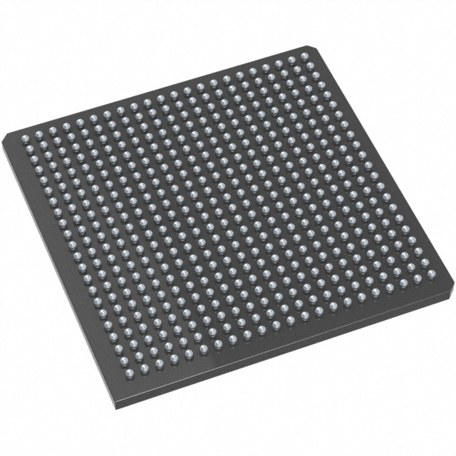
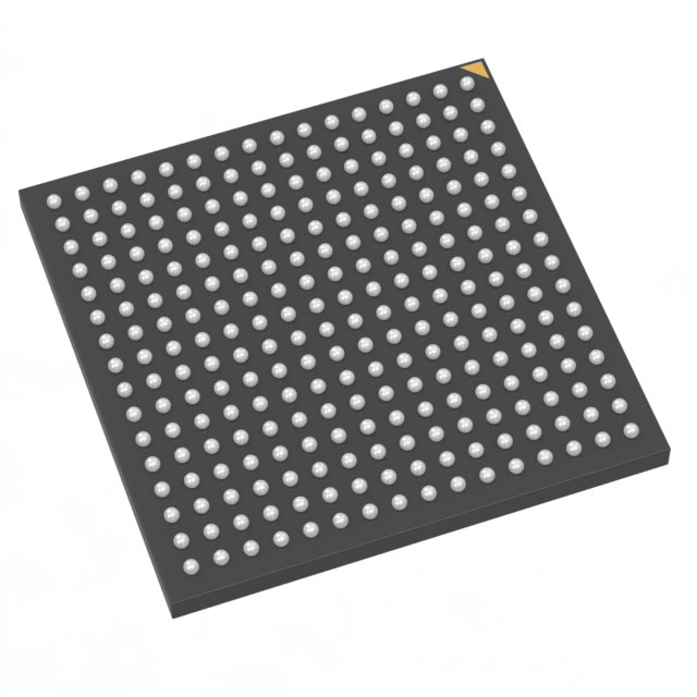
| Package / Case | 256-LBGA | Number of I/O | 119 | Voltage | 1.425 V - 1.575 V | ||
| Mounting Method | Surface Mount | RoHS Compliance | RoHS non-compliant | REACH Compliance | REACH Unaffected | ||
| Moisture Sensitivity Level | 3 (168 Hours) | Number of LABs/CLBs | 13824 | Number of Logic Elements/Cells | 13824 | ||
| Number of Gates | 600000 | ECCN | 3A991D | HTS Code | 8542.39.0001 | ||
| Qualification | N/A | Total RAM Bits | 110592 |
Overview of M7AFS600-1FG256I – Fusion® Field Programmable Gate Array (FPGA) IC, 119 I/Os, 110,592 bits, 256-LBGA
The M7AFS600-1FG256I is a Fusion® family mixed-signal, flash-based FPGA from Microchip Technology. It combines reprogrammable digital logic with integrated analog peripherals and MOSFET gate-driver capability to address industrial embedded applications that require on-chip analog acquisition, control and nonvolatile configuration.
Designed for industrial temperature operation, this device offers 600,000 system gates, 13,824 logic elements and approximately 108 kbits (110,592 bits) of embedded RAM in a 256-LBGA package, delivering a compact, integrated platform for mixed-signal designs.
Key Features
- Core and Logic – 600,000 system gates and 13,824 logic elements provide substantial programmable logic capacity for control, signal processing and glue-logic functions.
- Embedded Memory – Approximately 108 kbits (110,592 bits) of on-chip RAM plus Fusion-family embedded flash memory blocks (family listing indicates multi-megabit flash options) for configuration and data buffering.
- Analog and Mixed-Signal Integration – Integrated ADCs with up to 12-bit resolution and rates to 600 ksps, up to 30 analog input channels, internal/external reference options, current and temperature monitor blocks and high-voltage input tolerance (–10.5 V to +12 V).
- MOSFET Gate Drivers – Up to 10 programmable MOSFET gate-driver outputs with selectable drive strengths (including μA and 20 mA settings) to directly support power-stage control.
- I/O Flexibility – 119 I/Os with bank-selectable voltages (1.5 V, 1.8 V, 2.5 V, 3.3 V) and support for single-ended and differential standards (LVTTL/LVCMOS, LVPECL, LVDS, B-LVDS, M-LVDS) to interface with a wide range of peripherals and transceivers.
- Clocking and Timing – Internal 100 MHz RC oscillator, crystal support (32 kHz–20 MHz), programmable real-time counter and multiple clock-conditioning circuits with integrated PLLs for flexible clock synthesis and distribution.
- Power and Low-Power Modes – Core supply range specified at 1.425 V to 1.575 V; Fusion family devices support single 3.3 V I/O supply with an on-chip 1.5 V regulator and low-power standby modes.
- Security and In-System Programming (ISP) – ISP via JTAG with AES-128 support and FlashLock® protection to secure configuration and enable field updates.
- Package and Reliability – Surface-mount 256-LBGA (supplier package 256-FPBGA, 17×17), industrial grade with an operating temperature range of –40 °C to 85 °C and RoHS compliant.
Typical Applications
- Industrial Control and Power Conversion – Integrated MOSFET gate drivers and analog monitoring make the device suitable for power-stage control, motor-drive interfaces and industrial power-management subsystems.
- Sensor Acquisition and Conditioning – On-chip ADCs, multiple analog input channels and high-voltage-tolerant inputs enable compact sensor front-ends and data-acquisition systems.
- Mixed-Signal Embedded Systems – Flash-based nonvolatile configuration, embedded RAM and flexible I/O support instant-on operation and in-system updates for embedded controllers and instrumentation.
- Interface Aggregation and Custom I/O – 119 multi-voltage I/Os with differential capability allow consolidation of protocol bridges, timing logic and I/O buffering in communication and control platforms.
Unique Advantages
- Highly Integrated Mixed-Signal Platform: On-chip ADCs, analog I/O and MOSFET gate drivers reduce external component count and simplify PCB design.
- Nonvolatile Flash-Based FPGA: Retains configuration when powered off for instant-on operation and supports secure in-system programming.
- Flexible I/O Standards: Bank-selectable voltages and multiple single-ended/differential standards enable direct interfacing with diverse peripherals and transceivers.
- Industrial Temperature Rating: Specified operation from –40 °C to 85 °C for deployment in industrial environments.
- Scalable within Fusion Family: Compatibility across Fusion packages allows designers to scale logic, memory and analog resources while maintaining board-level reuse where applicable.
Why Choose M7AFS600-1FG256I?
The M7AFS600-1FG256I positions itself as an industrial-grade, mixed-signal FPGA that brings digital logic, embedded memory, analog acquisition and gate-driving capability into a single, surface-mount 256-LBGA device. Its combination of 600k system gates, 13,824 logic elements and a comprehensive analog peripheral set makes it well suited to compact, integrated control and data-acquisition applications where reducing BOM and board area matters.
For engineering teams targeting industrial embedded designs that require nonvolatile configuration, flexible I/O and on-chip analog resources, this Fusion-family device delivers an integrated platform with secure ISP, programmable clocking and robust operating-temperature support to help streamline development and long-term deployment.
Request a quote or submit an inquiry to receive pricing, availability and lead-time information for the M7AFS600-1FG256I.


Date Founded: 1989
Headquarters: Chandler, Arizona, USA
Employees: 22,000+
Revenue: $8.349 Billion
Certifications and Memberships: ISO9001:2015, IATF16949:2016, AS 9100D


