
XC4005-5PC84C
| Part Description |
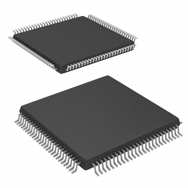
XC4000 Field Programmable Gate Array (FPGA) IC 61 6272 466 84-LCC (J-Lead) |
|---|---|
| Quantity | 209 Available (as of October 7, 2026) |

| Product Category | Field Programmable Gate Array (FPGA) |
|---|---|
| Manufacturer | AMD |
| Manufacturing Status | Obsolete |
| Manufacturer Standard Lead Time | Contact Us |
| Datasheet |
Specifications & Environmental
| Device Package | 84-PLCC (29.31x29.31) | Grade | Commercial | Operating Temperature | 0°C – 85°C | ||
|---|---|---|---|---|---|---|---|
| Package / Case | 84-LCC (J-Lead) | Number of I/O | 61 | Voltage | 4.75 V - 5.25 V | ||
| Mounting Method | Surface Mount | RoHS Compliance | RoHS non-compliant | REACH Compliance | REACH Unaffected | ||
| Moisture Sensitivity Level | 3 (168 Hours) | Number of LABs/CLBs | 196 | Number of Logic Elements/Cells | 466 | ||
| Number of Gates | 5000 | ECCN | EAR99 | HTS Code | 8542.39.0001 | ||
| Qualification | N/A | Total RAM Bits | 6272 |
Overview of XC4005-5PC84C – XC4000 Field Programmable Gate Array (84‑LCC J‑Lead, 61 I/O)
The XC4005-5PC84C is a field-programmable gate array (FPGA) from AMD's XC4000 family, featuring a regular array of configurable logic blocks surrounded by programmable I/O. It provides on-chip RAM and dedicated routing resources for custom digital logic and system control functions.
With 466 logic elements (cells), approximately 6,272 bits of embedded RAM, and 61 I/O pins in an 84‑lead LCC (J‑Lead) package, the device is well suited for development, prototyping and medium-density custom logic where reprogrammability and flexible I/O are required.
Key Features
- Configurable Logic Core — 466 logic elements (cells) arranged across 196 configurable logic blocks (CLBs) to implement custom logic functions.
- On‑chip RAM — Approximately 6,272 bits of embedded RAM for intermediate data storage and small buffering tasks inside the fabric.
- Gate‑equivalent Density — Approximately 5,000 gates of logic capacity for mid‑range logic integration.
- I/O and Packaging — 61 user I/O pins in an 84‑lead LCC (J‑Lead) surface‑mount package; supplier device package listed as 84‑PLCC (29.31 × 29.31 mm).
- Power and Thermal — Standard 5 V supply range (4.75 V to 5.25 V) and commercial operating temperature range of 0 °C to 85 °C.
- Programmability and Configuration — Devices in the XC4000 family are configured by loading a binary configuration file and support multiple programming modes with unlimited reprogrammability.
- Architecture Highlights (XC4000 family) — CLBs include independent 4‑input function generators and a combined-function generator, dedicated fast carry propagation, wide edge decoders, and an internal low‑skew global clock/signal distribution network.
- Assembly and Compliance — Surface‑mount mounting type and RoHS compliant.
Typical Applications
- Prototype and Development — Rapidly implement and iterate custom digital designs using the FPGA’s reprogrammability and on‑chip RAM for early system validation.
- Glue Logic and Interface Bridging — Consolidate discrete logic and translate between peripherals using the device’s mix of logic elements and 61 I/O pins.
- Configurable System Control — Implement control, sequencing, and peripheral management functions that benefit from in-field updates and iterative tuning.
Unique Advantages
- Reprogrammable Hardware: Unlimited reprogramming simplifies design iterations and allows hardware function updates without changing the PCB.
- Balanced Logic and I/O: 466 logic elements with 61 I/O pins provide a good balance for medium‑complexity logic and peripheral interfacing, reducing BOM by integrating functions on a single device.
- Embedded Memory: Approximately 6,272 bits of on‑chip RAM enable local data buffering and small LUT‑based RAM implementations.
- Standard 5 V Operation: Operates from 4.75 V to 5.25 V, compatible with common legacy and TTL‑level systems.
- Commercial Temperature Range: Rated for 0 °C to 85 °C for reliable operation in standard commercial environments.
- RoHS Compliant: Meets RoHS requirements for environmentally conscious production processes.
Why Choose XC4005-5PC84C?
The XC4005-5PC84C positions itself as a flexible, reprogrammable solution for engineers needing mid‑density FPGA capability in a compact 84‑lead package. Its combination of logic resource count, embedded RAM, and 61 I/O pins makes it well suited for developers and system integrators who require in‑field configurability and iterative design workflows.
Supported by the XC4000 family architecture and development tool ecosystem, the device offers a practical path from prototype to production volumes where programmable hardware and moderate integration density are required.
Request a quote or submit a quote today to check availability and pricing for the XC4005-5PC84C.
























Date Founded: 1969
Headquarters: Santa Clara, California, USA
Employees: 25,000+
Revenue: $22.68 Billion
Certifications and Memberships: ISO9001:2015, RoHS, REACH











