
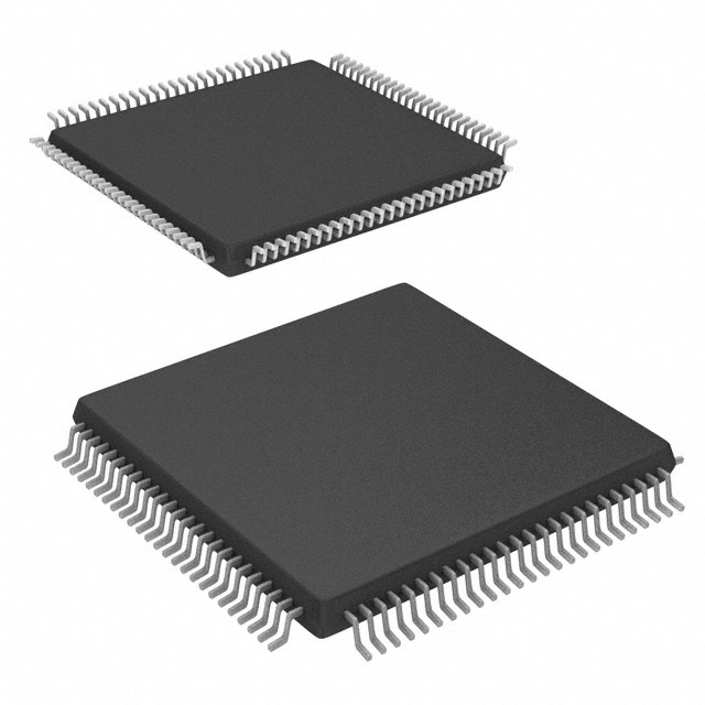
XC4005-5PQ160C
| Part Description |
XC4000 Field Programmable Gate Array (FPGA) IC 112 6272 466 160-BQFP |
|---|---|
| Quantity | 517 Available (as of October 8, 2026) |

| Product Category | Field Programmable Gate Array (FPGA) |
|---|---|
| Manufacturer | AMD |
| Manufacturing Status | Obsolete |
| Manufacturer Standard Lead Time | Contact Us |
| Datasheet |
Specifications & Environmental
| Device Package | 160-PQFP (28x28) | Grade | Commercial | Operating Temperature | 0°C – 85°C | ||
|---|---|---|---|---|---|---|---|
| Package / Case | 160-BQFP | Number of I/O | 112 | Voltage | 4.75 V - 5.25 V | ||
| Mounting Method | Surface Mount | RoHS Compliance | RoHS non-compliant | REACH Compliance | REACH Unaffected | ||
| Moisture Sensitivity Level | 3 (168 Hours) | Number of LABs/CLBs | 196 | Number of Logic Elements/Cells | 466 | ||
| Number of Gates | 5000 | ECCN | EAR99 | HTS Code | 8542.39.0001 | ||
| Qualification | N/A | Total RAM Bits | 6272 |
Overview of XC4005-5PQ160C – XC4000 Field Programmable Gate Array (FPGA) IC 112 6272 466 160-BQFP
The XC4005-5PQ160C is a commercial-grade Field Programmable Gate Array (FPGA) from AMD based on the XC4000 family architecture. It combines a regular array of Configurable Logic Blocks (CLBs) and a perimeter of programmable Input/Output Blocks (IOBs) with on-chip memory and flexible routing to implement custom digital logic.
With 196 CLBs (466 logic elements), approximately 6,272 bits of on-chip RAM, 112 user I/Os and a 160-BQFP surface-mount package, this device targets reprogrammable logic applications where design flexibility, integration and standard 5 V system compatibility are required.
Key Features
- Core Architecture Configurable Logic Blocks (196 CLBs) and 466 logic elements provide a flexible programmable fabric for implementing custom digital functions.
- On-Chip Memory Approximately 6,272 bits of embedded RAM for local state storage and fast data buffering inside the CLB fabric.
- I/O Density 112 programmable I/Os arranged around the device perimeter for connecting to a wide range of external logic and peripherals.
- Performance-Oriented Logic Third-generation FPGA features from the XC4000 family including abundant flip-flops, flexible function generators, a dedicated high-speed carry-propagation circuit and wide edge decoders.
- Clock and Routing Resources Hierarchy of interconnect lines and an eight-node global low-skew clock/signal distribution network to support synchronous designs and complex interconnect patterns.
- Configuration Flexibility Device is configured by loading a binary configuration file into internal memory cells; supports multiple programming modes and unlimited reprogrammability as part of the XC4000 family.
- Package & Mounting 160-BQFP (supplier device package 160-PQFP, 28 × 28 mm) surface-mount package for PCB integration in compact board layouts.
- Power & Temperature Single-supply operation at 4.75 V to 5.25 V and commercial operating temperature range of 0 °C to 85 °C.
- Standards & Compliance RoHS-compliant lead-free construction.
Typical Applications
- Reconfigurable Prototyping: Used to implement and iterate custom logic during hardware development cycles where on-the-fly reprogramming accelerates design validation.
- Custom Digital Functions: Implement glue logic, protocol translators or bespoke combinational/sequential circuits leveraging the device's CLB fabric and on-chip RAM.
- Board-Level Integration with Boundary-Scan: Supports system designs that require IEEE 1149.1-compatible boundary-scan features for test and bring-up workflows.
- Mid-Volume Production: Suitable for production designs where the benefits of reprogrammability and integration outweigh fixed-mask ASIC approaches.
Unique Advantages
- Flexible, Reprogrammable Hardware: Unlimited reprogrammability lets designs evolve without PCB redesigns, shortening development cycles and enabling in-field updates.
- Integrated Logic and Memory: The combination of 196 CLBs and embedded RAM simplifies designs by keeping critical logic and temporary data on-chip, reducing external component count.
- High I/O Count in a Compact Package: 112 I/Os in a 160-BQFP package provide a balance of connectivity and board space efficiency for complex designs.
- Established XC4000 Feature Set: Third-generation FPGA features such as high-speed carry circuits, function generators and wide decoders help implement arithmetic and control logic efficiently.
- Standard 5 V Compatibility: Operates from 4.75 V to 5.25 V power rails common in many legacy and mixed-voltage systems.
- RoHS Compliance: Meets lead-free assembly requirements for modern manufacturing flows.
Why Choose XC4005-5PQ160C?
The XC4005-5PQ160C brings the XC4000 family’s programmable logic architecture into compact, surface-mount form with a clear set of capabilities: 196 CLBs (466 logic elements), on-chip RAM, 112 I/Os and a 160-BQFP footprint. It is positioned for designers who need reprogrammable logic, moderate on-chip memory and strong I/O integration within standard 5 V commercial systems.
Backed by the XC4000 family’s development ecosystem and configuration modes, the XC4005-5PQ160C delivers a scalable, reprogrammable platform for prototyping, custom digital implementations and mid-volume production where flexibility and integration reduce BOM complexity and support faster time-to-market.
Request a quote or submit an inquiry to get pricing, availability and technical support for the XC4005-5PQ160C.






















Date Founded: 1969
Headquarters: Santa Clara, California, USA
Employees: 25,000+
Revenue: $22.68 Billion
Certifications and Memberships: ISO9001:2015, RoHS, REACH











