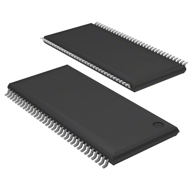
AS4C8M16D1-5TIN
| Part Description |
IC DRAM 128MBIT PAR 66TSOP II |
|---|---|
| Quantity | 1,415 Available (as of June 10, 2026) |
| Product Category | Memory |
|---|---|
| Manufacturer | Alliance Memory, Inc. |
| Manufacturing Status | Obsolete |
| Manufacturer Standard Lead Time | Contact Us |
| Datasheet |
Specifications & Environmental
| Device Package | 66-TSOP II | Memory Format | DRAM | Technology | SDRAM - DDR | ||
|---|---|---|---|---|---|---|---|
| Memory Size | 128 Mbit | Access Time | 700 ps | Grade | Industrial | ||
| Clock Frequency | 200 MHz | Voltage | 2.3V ~ 2.7V | Memory Type | Volatile | ||
| Operating Temperature | -40°C ~ 85°C (TA) | Write Cycle Time Word Page | 15 ns | Packaging | 66-TSSOP (0.400", 10.16mm Width) | ||
| Mounting Method | Volatile | Memory Interface | Parallel | Memory Organization | 8M x 16 | ||
| Moisture Sensitivity Level | 3 (168 Hours) | RoHS Compliance | ROHS3 Compliant | REACH Compliance | REACH Unaffected | ||
| Qualification | N/A | ECCN | 3A991B2A | HTS Code | 8542.32.0002 |
Overview of AS4C8M16D1-5TIN – IC DRAM 128MBIT PAR 66TSOP II
The AS4C8M16D1-5TIN is a 128 Mbit DDR1 synchronous DRAM organized as 8M × 16 from Alliance Memory, Inc. It implements a parallel DDR interface with internal pipelined architecture and four internal banks for burst-oriented read/write access.
Designed for applications that require high memory bandwidth and predictable timing, this device delivers 200 MHz clock operation with programmable burst lengths and mode registers, packaged in a 66-pin TSOP II suitable for industrial temperature environments.
Key Features
- Core / Memory Architecture 128 Mbit DDR SDRAM arranged as 8M × 16 (quad 2M × 16 banks), supporting burst-oriented read and write accesses.
- Performance Fast clock rate up to 200 MHz and an access time of 700 ps; write cycle time (word/page) of 15 ns.
- DDR Functionality Double data rate operation with data outputs on both rising edges of CK/CK; differential clock inputs and bi-directional DQS for data strobe timing.
- Programmability & Burst Control Programmable Mode and Extended Mode registers with CAS latencies of 2, 2.5, 3 and selectable burst lengths of 2, 4, or 8 (sequential or interleaved).
- Power & I/O Low-voltage operation with VDD & VDDQ = 2.5V ±5% (specified voltage range 2.3 V to 2.7 V) and SSTL_2 I/O interface.
- Power Management & Reliability Auto Refresh and Self Refresh support with 4096 refresh cycles per 64 ms, plus precharge and active power-down modes.
- Package & Temperature 66-pin TSOP II (66-TSSOP, 0.400" / 10.16 mm width) package rated for industrial operation from −40°C to 85°C (TA).
- Compliance Indicators Datasheet notes Pb free and Halogen free construction for this DDR SDRAM variant.
Typical Applications
- High-bandwidth memory subsystems Well suited for designs requiring high memory bandwidth and predictable burst access patterns.
- Industrial temperature systems Use in equipment that must operate across −40°C to 85°C ambient temperature ranges.
- Parallel-interface memory expansion Integration where a parallel DDR SDRAM with SSTL_2 I/O and TSOP II footprint is required.
Unique Advantages
- Industrial temperature rating: Specified operation from −40°C to 85°C supports deployments in temperature-critical environments.
- 200 MHz DDR operation: Double data-rate transfers at a 200 MHz clock provide increased throughput for burst accesses.
- Flexible timing and burst options: CAS latencies (2 / 2.5 / 3) and burst lengths (2, 4, 8) plus programmable mode registers allow tuning for system timing and performance.
- Robust refresh and power features: Auto and self refresh plus power-down modes and 4096 refresh cycles/64 ms support reliable data retention and power management.
- Industry-standard package: 66-pin TSOP II (0.65 mm pin pitch) offers a compact footprint compatible with existing TSOP II board designs.
- Low-voltage operation: VDD/VDDQ = 2.5V ±5% (2.3 V to 2.7 V) reduces supply requirements for DDR memory subsystems.
Why Choose AS4C8M16D1-5TIN?
The AS4C8M16D1-5TIN provides a compact, industrial-temperature DDR1 memory option with configurable burst and timing settings for predictable high-bandwidth performance. Its quad-bank architecture, differential clocking, bi-directional DQS and SSTL_2 interface make it suitable where synchronous, burst-oriented memory is required.
Engineers designing systems that demand stable operation across wide temperature ranges, controlled timing options, and a TSOP II footprint will find this 128 Mbit DDR SDRAM a practical building block. The device's refresh, power-down, and programmability features support long-term robustness and integration into established parallel-memory designs.
Request a quote or submit a sourcing inquiry for AS4C8M16D1-5TIN to obtain pricing, lead time, or additional technical information.