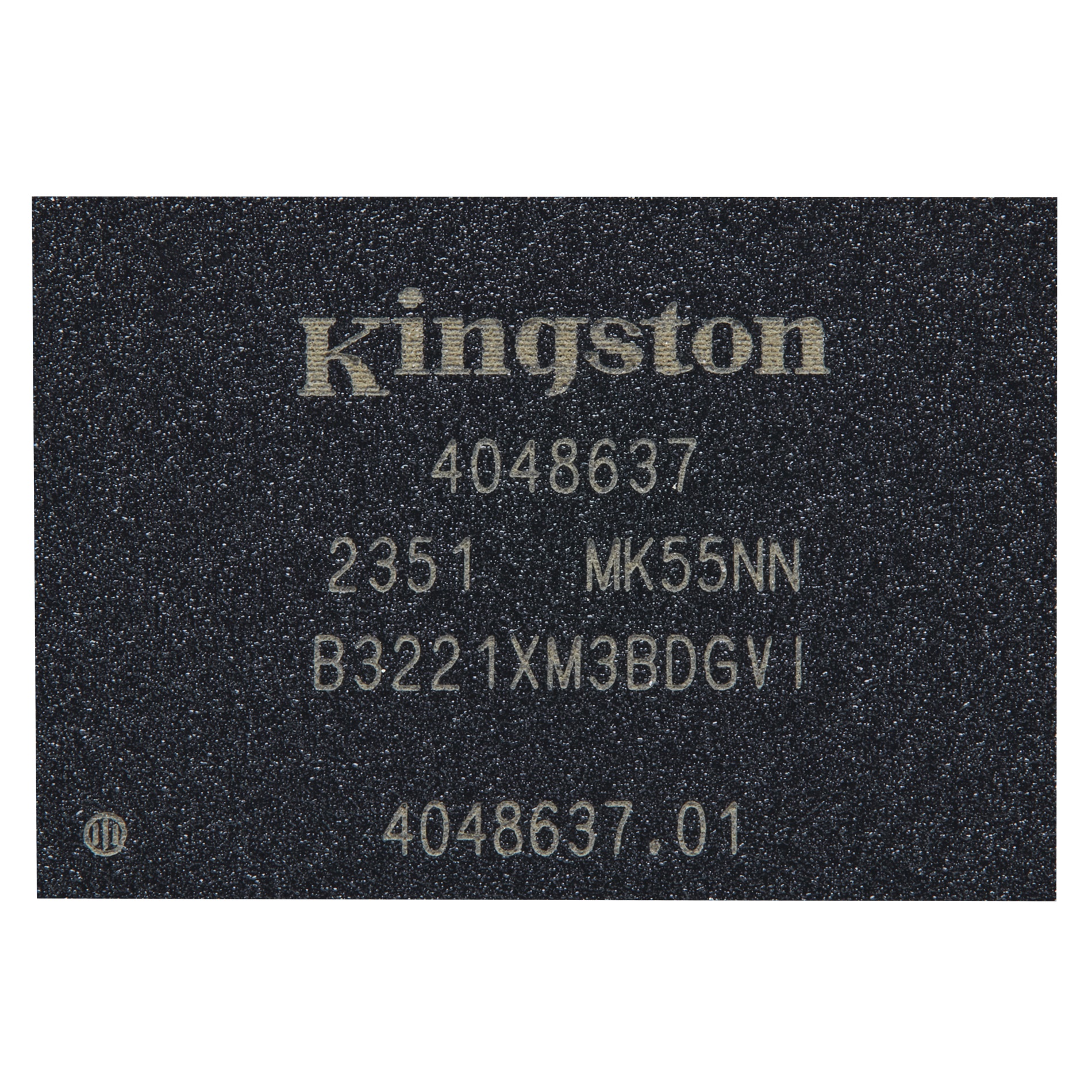
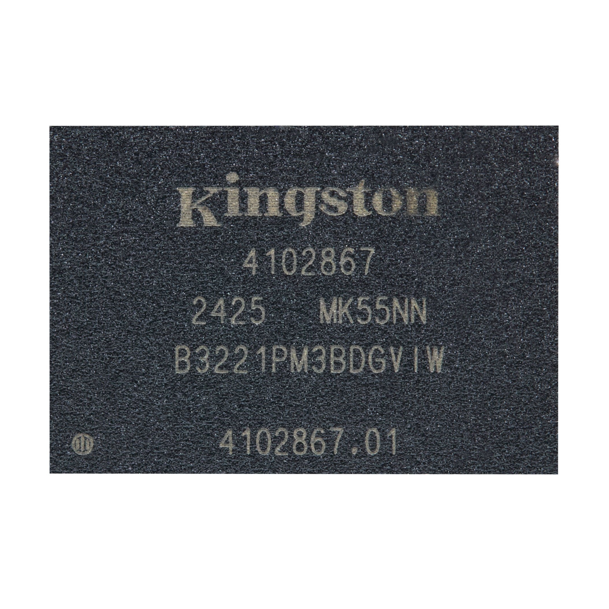
B3221PM3BDGVIW-U
| Part Description |
32GB 200 BALL LPDDR4 4266MH |
|---|---|
| Quantity | 1,393 Available (as of June 15, 2026) |
| Product Category | Memory |
|---|---|
| Manufacturer | Kingston Technology |
| Manufacturing Status | Active |
| Manufacturer Standard Lead Time | 24 Weeks |
| Datasheet |
Specifications & Environmental
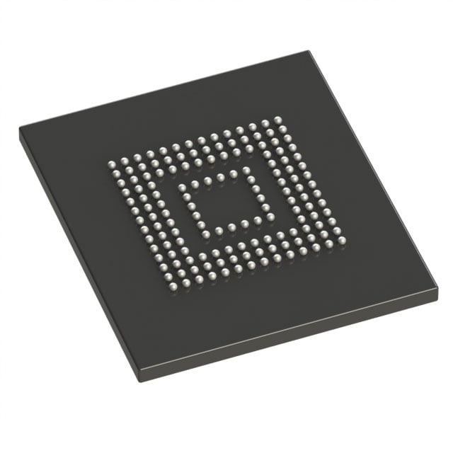
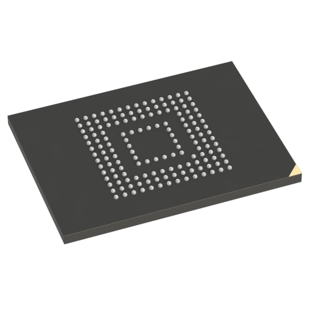
| Device Package | 200-FBGA (10x14.5) | Memory Format | DRAM | Technology | SDRAM - Mobile LPDDR4 | ||
|---|---|---|---|---|---|---|---|
| Memory Size | 32 Gbit | Access Time | 3.5 ns | Grade | Automotive | ||
| Clock Frequency | 2.133 GHz | Voltage | 1.06V ~ 1.17V, 1.7V ~ 1.95V | Memory Type | Volatile | ||
| Operating Temperature | -40°C ~ 95°C (TC) | Write Cycle Time Word Page | 18 ns | Packaging | 200-WFBGA | ||
| Mounting Method | Volatile | Memory Interface | Parallel | Memory Organization | 2G x 16 | ||
| Moisture Sensitivity Level | 3 (168 Hours) | RoHS Compliance | Unknown | REACH Compliance | REACH Unknown | ||
| Qualification | N/A | ECCN | EAR99 | HTS Code | 8542.32.0036 |
Overview of B3221PM3BDGVIW-U – 32GB 200 BALL LPDDR4 4266MH
The B3221PM3BDGVIW-U is a mobile LPDDR4 SDRAM device in a 200-ball FBGA package that delivers up to 4266 Mb/s data rate. It implements a two-die 16Gbit configuration to provide a 32 Gbit DRAM device organized as 1024M x 16 x 2 channels with a parallel memory interface.
Designed for low-power mobile-class applications, the device combines DRAM features such as per-bank refresh, programmable latencies and burst lengths, and differential clocks to address designs that require compact, high-bandwidth, low-voltage memory with extended temperature capability.
Key Features
- Memory Architecture — 32 Gbit device composed of two 16 Gbit (x16) die in one package; organization shown as 1024M ×16 ×2 channels and 8 internal banks per channel.
- High Data Rate — Supports data rates up to 4266 Mbps (double-data-rate architecture with two transfers per clock) with a clock frequency listed at 2.133 GHz.
- Burst and Latency Options — Burst lengths 16, 32 and on-the-fly (MRS-enabled); programmable read and write latencies and programmable driver strength for timing optimization.
- Low-Voltage Operation — Dual supply domains: VDD1 = 1.8 V (1.70–1.95 V) and VDD2/VDDCA/VDDQ = 1.1 V (1.06–1.17 V), enabling low-power operation.
- Refresh and Power Management — Supports auto-refresh, self-refresh, per-bank refresh, partial array self-refresh (PASR), bank masking and segment masking; built-in temperature sensor for auto temperature-compensated self-refresh (ATCSR).
- Interface and Signal Integrity — Differential clock inputs (CK_t/CK_c) and bi-directional differential data strobe (DQS_t/DQS_c); DMI pin support for write data masking and DBIdc functionality.
- Compact Package — 200-ball FBGA package (10 × 14.5 mm) suitable for space-constrained board designs.
- Extended Temperature Range — Industrial temperature option rated from −40°C to +95°C (TC) for deployments requiring wider operating range.
- Performance Characteristics — Access time of 3.5 ns and write cycle time (word page) of 18 ns as specified.
Typical Applications
- Mobile Devices — Mobile LPDDR4 technology and high data rate make it suitable for memory subsystems in handheld and mobile platforms that require compact, low-power DRAM.
- Low-Power Embedded Systems — Low-voltage operation and self-refresh/PASR features support embedded designs that prioritize power efficiency and memory retention.
- Industrial Equipment — Availability with an industrial temperature range (−40°C to +95°C TC) supports designs operating in extended-temperature environments.
Unique Advantages
- High-bandwidth LPDDR4 performance: Up to 4266 Mbps data rate with DDR architecture to support bandwidth-sensitive memory operations.
- Scalable density in a single package: Two 16 Gbit die combined to deliver 32 Gbit density without larger package footprints.
- Power-efficient operation: Dual supply domains and self-refresh/PASR reduce runtime and retention power for battery- or energy-constrained designs.
- Flexible timing and signaling: Programmable RL/WL, programmable driver strength, and on-the-fly burst mode enable tuning for system timing and signal-integrity requirements.
- Robust refresh control: Per-bank refresh, bank/segment masking and ATCSR provide granular refresh strategies to optimize performance and power.
- Compact FBGA package: 200-ball FBGA (10 × 14.5 mm) enables high-density board placement while supporting parallel memory interface requirements.
Why Choose B3221PM3BDGVIW-U?
The B3221PM3BDGVIW-U is a Kingston Technology LPDDR4 DRAM device designed to combine high data throughput (up to 4266 Mbps) with low-voltage operation and compact 200-ball FBGA packaging. Its architecture—two 16 Gbit die in one package with 8 banks per channel, programmable latencies, and advanced refresh features—addresses designs that need dense, configurable mobile-class memory.
This device is suited to engineers specifying LPDDR4 memory for mobile, low-power embedded, and industrial-temperature applications that require precise timing control, granular refresh management, and a small board footprint.
Request a quote or contact sales to discuss pricing, availability, and qualification options for the B3221PM3BDGVIW-U.