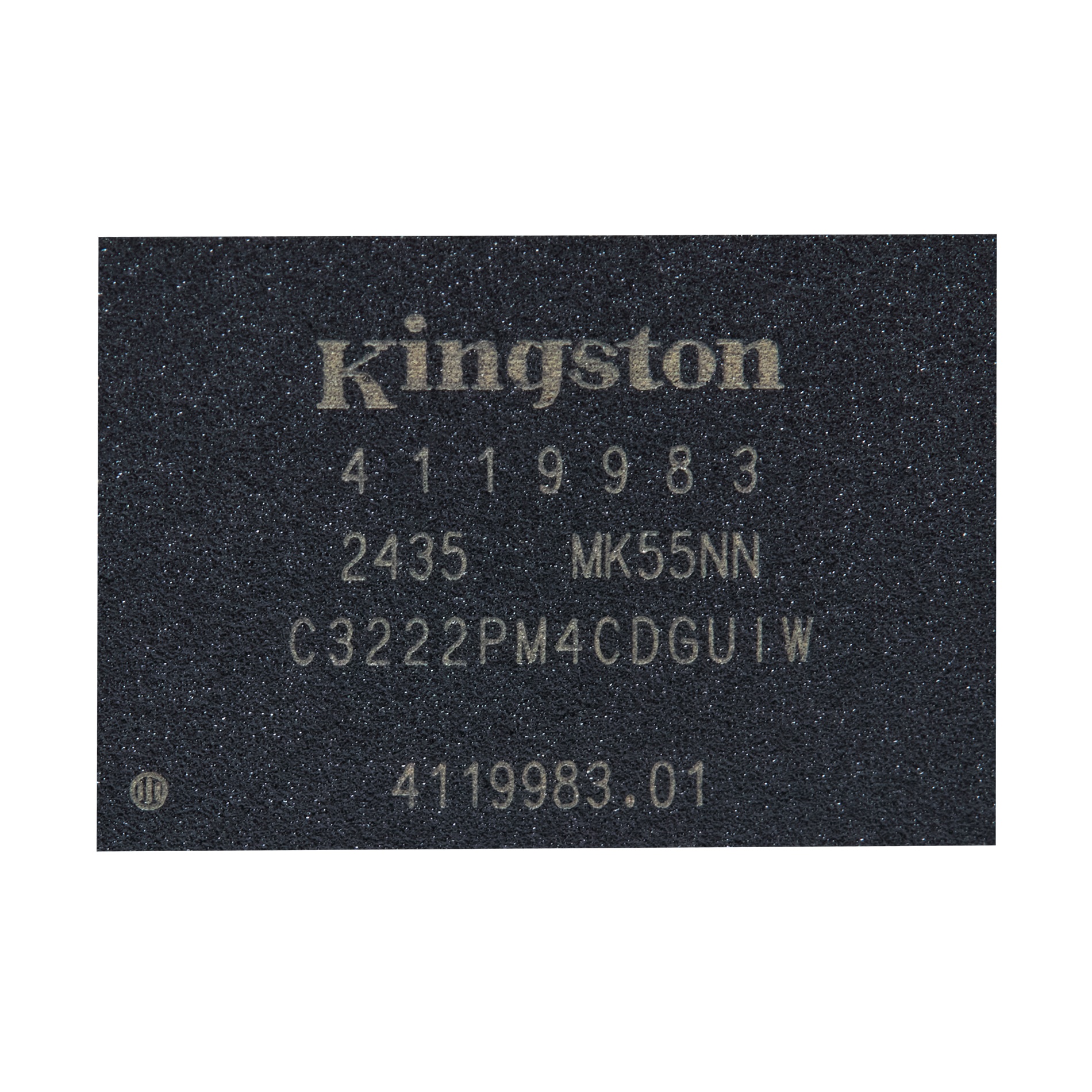
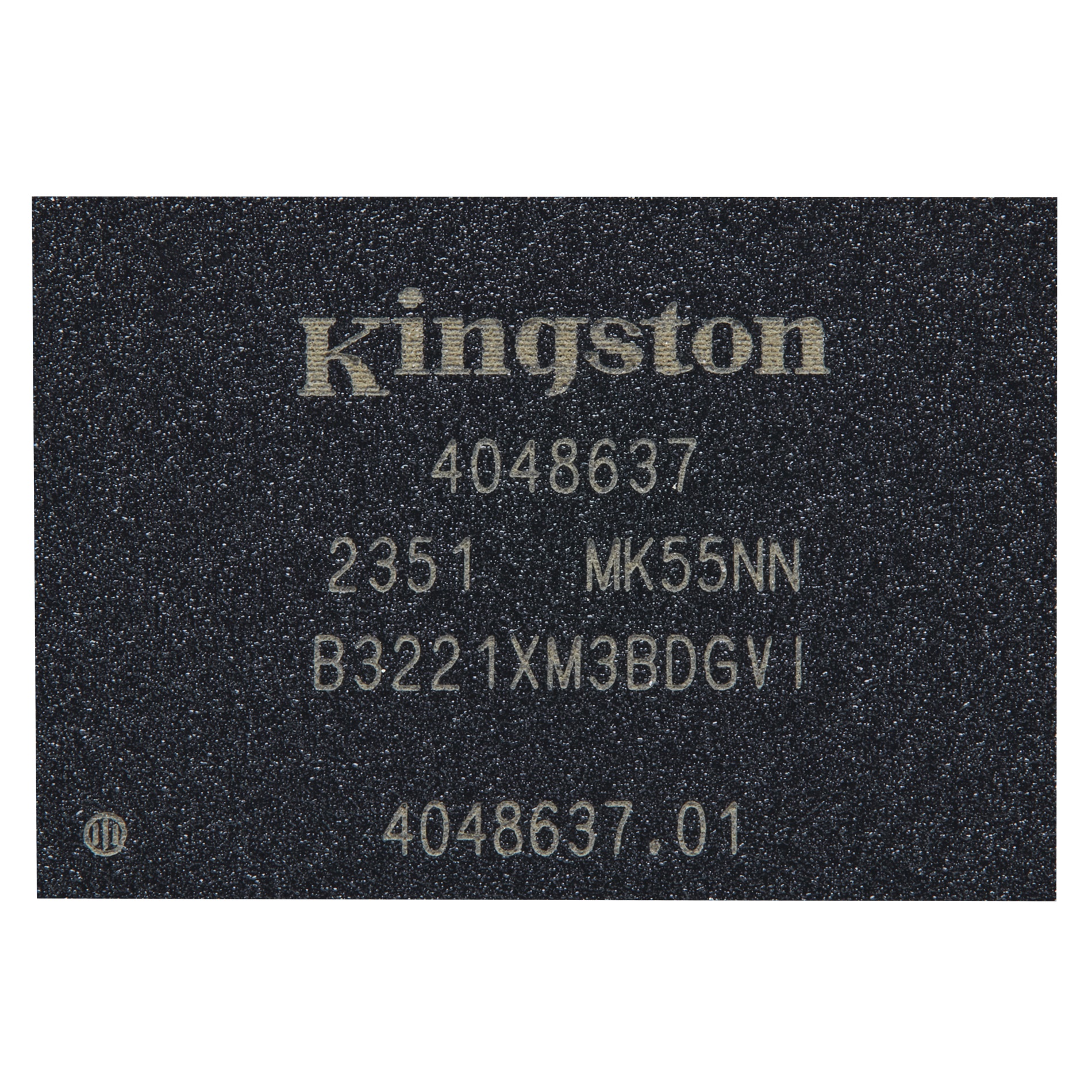
B3221XM3BDGVI-U
| Part Description |
IC DRAM 32GBIT PAR 200FBGA |
|---|---|
| Quantity | 769 Available (as of June 10, 2026) |
| Product Category | Memory |
|---|---|
| Manufacturer | Kingston Technology |
| Manufacturing Status | Active |
| Manufacturer Standard Lead Time | 24 Weeks |
| Datasheet |
Specifications & Environmental
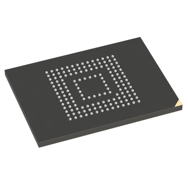
| Device Package | 200-FBGA (10x14.5) | Memory Format | DRAM | Technology | SDRAM - Mobile LPDDR4X | ||
|---|---|---|---|---|---|---|---|
| Memory Size | 32 Gbit | Access Time | 3.5 ns | Grade | Industrial | ||
| Clock Frequency | 2.133 GHz | Voltage | 1.06V ~ 1.17V, 1.7V ~ 1.95V | Memory Type | Volatile | ||
| Operating Temperature | -25°C ~ 85°C (TC) | Write Cycle Time Word Page | 18 ns | Packaging | 200-WFBGA | ||
| Mounting Method | Volatile | Memory Interface | Parallel | Memory Organization | 2G x 16 | ||
| Moisture Sensitivity Level | 3 (168 Hours) | RoHS Compliance | ROHS3 Compliant | REACH Compliance | REACH Unknown | ||
| Qualification | N/A | ECCN | EAR99 | HTS Code | 8542.32.0036 |
Overview of B3221XM3BDGVI-U – IC DRAM 32GBIT PAR 200FBGA
The B3221XM3BDGVI-U is a 32 Gbit low-power DRAM device in an LPDDR4X architecture, delivered in a 200-ball FBGA package. It combines dual-channel x16 organization with high data-rate operation and low-voltage power rails for mobile and low-power memory subsystems.
Designed for applications that require high-throughput, low-power memory, this device offers programmable latency, advanced refresh and power-management features, and a compact FBGA footprint for space-constrained designs.
Key Features
- Memory Architecture — 1024M x 16 × 2 channels (32 Gbit total); organization supports two 16Gb die in one package for the 32Gb device.
- High Data Rate — Clock rate up to 2133 MHz yielding a per-pin data rate up to 4266 Mb/s (DDR), supporting burst lengths of 16, 32 and on-the-fly mode.
- Banking and Concurrency — Eight internal banks per channel enable concurrent operation across banks to improve throughput.
- Programmable Timing — Read and write latencies (RL/WL) are programmable; example timing includes a write cycle time (word page) of 18 ns and an access time of 3.5 ns.
- Advanced Refresh & Power Management — Supports auto-refresh, self-refresh, per-bank refresh, partial array self-refresh (PASR), bank masking, segment masking and auto temperature compensated self-refresh (ATCSR) via built-in temperature sensor; 8192 refresh cycles per 32 ms.
- Low-Voltage Operation — Multi-rail supply: VDD1 = 1.80V (1.70–1.95V), VDD2 = 1.10V (1.06–1.17V), VDDQ = 0.60V (0.57–0.65V) for reduced power consumption.
- Interface and Signaling — Differential clock inputs (CK_t/CK_c) and bi-directional differential data strobe (DQS_t/DQS_c); commands and data referenced to differential edges with DBI/DMI support for data masking.
- Package and Thermal — 200-ball FBGA (200-WFBGA / supplier package: 200-FBGA 10 × 14.5 mm) with operating temperature range TC = −25°C to +85°C.
Typical Applications
- Mobile and Handheld Devices — Low-voltage LPDDR4X architecture and high per-pin data rates supply the memory bandwidth and power efficiency needed in mobile subsystems.
- Low-Power Embedded Systems — Self-refresh, PASR and ATCSR features reduce standby power and enable extended field operation in battery-powered designs.
- Compact Memory Modules — 200-ball FBGA package and dual-channel x16 organization support dense memory implementations in space-constrained boards and modules.
Unique Advantages
- High-throughput DDR Operation: Up to 4266 Mb/s per pin and burst-length flexibility for throughput-optimized transfers.
- Dual-channel x16 Integration: Two 16-bit channels in a single package deliver 32 Gbit density while simplifying board-level routing and BOM.
- Comprehensive Low-Power Features: PASR, ATCSR, self-refresh and per-bank refresh reduce active and standby energy use in power-sensitive applications.
- Programmable Latency and Driver Strength: RL/WL and driver strength are configurable to tune performance and signal integrity for specific system requirements.
- Robust Thermal Range: Rated for TC = −25°C to +85°C to match many industrial and commercial operating environments.
- Compact FBGA Footprint: 200-ball FBGA (10 × 14.5 mm) offers a small form factor for dense PCB layouts.
Why Choose B3221XM3BDGVI-U?
The B3221XM3BDGVI-U positions itself as a high-density, low-power LPDDR4X DRAM solution that balances bandwidth and energy efficiency for mobile and compact embedded memory subsystems. Its dual-channel x16 organization, programmable timing, and extensive refresh/power-management features make it suitable for designs that require configurable performance and reduced standby power.
This device is appropriate for engineering teams building space-constrained boards or modules that need 32 Gbit density with high per-pin data rates, configurable timing, and a proven set of low-power features. The compact 200-ball FBGA and broad voltage/temperature operating ranges support flexible integration into a variety of hardware platforms.
Request a quote or submit an inquiry for pricing and availability for the B3221XM3BDGVI-U.