IS25LX256-JHLA3-TR
| Part Description |
IC FLASH 256MBIT SPI/OCT 24TFBGA |
|---|---|
| Quantity | 356 Available (as of June 15, 2026) |

| Product Category | Memory |
|---|---|
| Manufacturer | Integrated Silicon Solution Inc |
| Manufacturing Status | Active |
| Manufacturer Standard Lead Time | 16 Weeks |
| Datasheet |
Specifications & Environmental
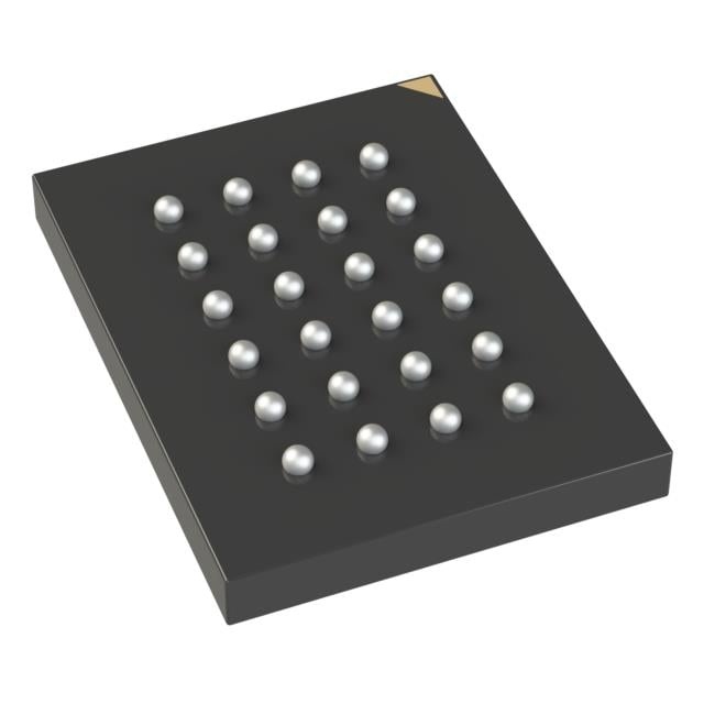
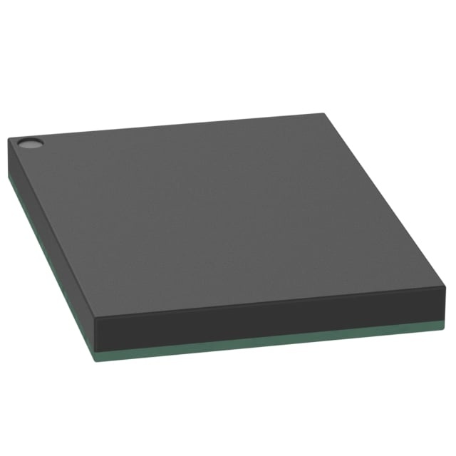
| Device Package | 24-TFBGA (6x8) | Memory Format | FLASH | Technology | FLASH | ||
|---|---|---|---|---|---|---|---|
| Memory Size | 256 Mbit | Access Time | N/A | Grade | Automotive | ||
| Clock Frequency | 133 MHz | Voltage | 2.7V ~ 3.6V | Memory Type | Non-Volatile | ||
| Operating Temperature | -40°C ~ 125°C (TA) | Write Cycle Time Word Page | N/A | Packaging | 24-TBGA | ||
| Mounting Method | Non-Volatile | Memory Interface | SPI - Octal I/O | Memory Organization | 32M x 8 | ||
| Moisture Sensitivity Level | 3 (168 Hours) | RoHS Compliance | ROHS3 Compliant | REACH Compliance | REACH Unaffected | ||
| Qualification | N/A | ECCN | 3A991B1A | HTS Code | 8542.32.0071 |
Overview of IS25LX256-JHLA3-TR - 256Mbit Octal SPI Flash Memory
The IS25LX256-JHLA3-TR is a 256-megabit NOR flash memory device from ISSI, featuring an advanced Octal SPI interface for high-speed serial communication. Organized as 32M x 8, this non-volatile memory combines the flexibility of SPI protocol with enhanced throughput via eight I/O lines, enabling data transfer rates up to 133MHz. Designed for embedded systems requiring fast boot times and reliable code storage, it delivers the performance and density needed for automotive, industrial, and consumer applications.
With an extended temperature range of -40°C to 125°C and a compact 24-TFBGA package, this flash memory provides robust storage in space-constrained designs operating in harsh environments.
Key Features
- High-Density Non-Volatile Storage - 256Mbit (32MB) of FLASH memory organized as 32M x 8, providing ample capacity for firmware, configuration data, and application code storage.
- Octal SPI Interface - Eight I/O lines enable significantly higher data throughput compared to standard Quad SPI, supporting clock frequencies up to 133MHz for faster read operations and reduced boot times.
- Wide Operating Voltage - 2.7V to 3.6V supply voltage range accommodates common system power rails and simplifies integration into 3V and 3.3V designs.
- Extended Temperature Range - Rated for -40°C to 125°C ambient operation, ensuring reliable performance in automotive, industrial control, and outdoor equipment.
- Compact TFBGA Package - 24-pin TFBGA (6mm x 8mm) footprint minimizes PCB space while providing efficient thermal characteristics for high-density board layouts.
Typical Applications
- Automotive Electronics - This flash memory serves as code storage for instrument clusters, body control modules, and infotainment systems where the extended temperature range ensures reliable operation across all climate conditions and the high-speed interface supports fast boot requirements.
- Industrial Control Systems - The device provides firmware storage for PLCs, motor drives, and HMI controllers where non-volatile retention is critical for configuration persistence and the wide temperature rating supports factory floor environments.
- IoT and Edge Computing - The compact package and low pin count make this memory ideal for space-constrained IoT gateways and edge devices that require fast code execution and reliable data logging capabilities.
- Consumer Electronics - Suitable for set-top boxes, smart home devices, and appliances that need efficient boot code storage and the flexibility of in-system programmability for firmware updates.
Unique Advantages
- Faster System Boot Times: The Octal SPI interface delivers up to twice the throughput of Quad SPI, reducing initialization delays in performance-critical applications.
- Simplified Pin Count: Serial interface architecture requires fewer pins than parallel flash, simplifying routing and reducing connector costs in multi-board systems.
- Extended Lifecycle Support: Active lifecycle status ensures long-term availability for designs with multi-year production horizons, reducing obsolescence risk.
- Proven Flash Technology: NOR flash architecture provides byte-level random access and high endurance, making it well-suited for execute-in-place (XIP) applications.
- Design Flexibility: Wide voltage range and temperature tolerance enable reuse across multiple product families without component substitution.
- Space Efficiency: Small TFBGA footprint maximizes available board area for additional functionality in miniaturized designs.
Why Choose IS25LX256-JHLA3-TR?
The IS25LX256-JHLA3-TR is engineered for designers who need reliable, high-speed non-volatile storage without the complexity of parallel interfaces or the cost of higher-density solutions. Its Octal SPI architecture bridges the gap between traditional Quad SPI and more complex memory technologies, delivering meaningful performance improvements with minimal design changes. The extended temperature rating and active lifecycle status make it particularly valuable for industrial and automotive designs requiring long-term component availability.
For systems where boot performance, code storage density, and environmental ruggedness are critical, the IS25LX256-JHLA3-TR provides a proven, cost-effective solution backed by ISSI's expertise in memory technology.
Get Started Today
Contact our sales team to discuss pricing, availability, and technical support for the IS25LX256-JHLA3-TR. Our specialists can help you evaluate whether this memory solution meets your design requirements and provide guidance on integration and programming.