IS42S32800B-7TI-TR
| Part Description |
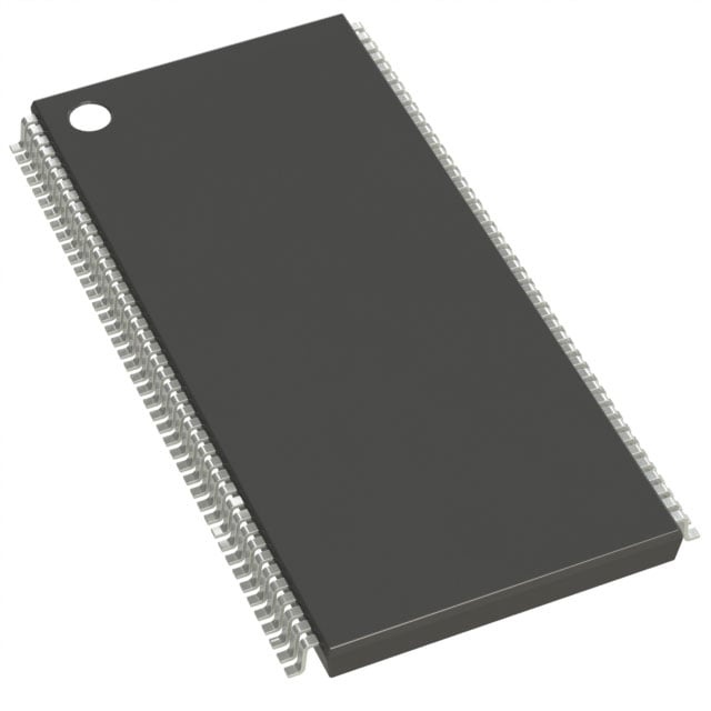
IC DRAM 256MBIT PAR 86TSOP II |
|---|---|
| Quantity | 225 Available (as of June 14, 2026) |

| Product Category | Memory |
|---|---|
| Manufacturer | Integrated Silicon Solution Inc |
| Manufacturing Status | Obsolete |
| Manufacturer Standard Lead Time | Contact Us |
| Datasheet |
Specifications & Environmental
| Device Package | 86-TSOP II | Memory Format | DRAM | Technology | SDRAM | ||
|---|---|---|---|---|---|---|---|
| Memory Size | 256 Mbit | Access Time | 5.5 ns | Grade | Industrial | ||
| Clock Frequency | 143 MHz | Voltage | 3V ~ 3.6V | Memory Type | Volatile | ||
| Operating Temperature | -40°C ~ 85°C (TA) | Write Cycle Time Word Page | N/A | Packaging | 86-TFSOP (0.400", 10.16mm Width) | ||
| Mounting Method | Volatile | Memory Interface | Parallel | Memory Organization | 8M x 32 | ||
| Moisture Sensitivity Level | 3 (168 Hours) | RoHS Compliance | ROHS3 Compliant | REACH Compliance | REACH Unaffected | ||
| Qualification | N/A | ECCN | EAR99 | HTS Code | 8542.32.0024 |
Overview of IS42S32800B-7TI-TR – IC DRAM 256MBIT PAR 86TSOP II
The IS42S32800B-7TI-TR is a 256‑Mbit synchronous DRAM (SDRAM) organized as quad 2M × 32 banks with a fully synchronous, registered-clock interface. It implements an internal pipelined architecture with programmable burst and mode options to support high‑bandwidth memory access patterns.
This device targets systems that require compact parallel SDRAM in an 86‑pin TSOP II package, offering selectable clock rates, CAS latencies, and refresh modes for designs that must balance performance and system-level integration.
Key Features
- Core & Memory Organization — Quad banks organized as 2M × 32 bits × 4 banks (2M words × 32 bits per bank) for a total of 256 Mbit.
- Performance — Supports clock rates of 166 MHz and 143 MHz with an access time listed at 5.5 ns and programmable CAS latency of 2 or 3 to tune read/write timing.
- Burst and Mode Flexibility — Programmable burst lengths of 1, 2, 4, 8 or full page, selectable burst type (interleaved or linear), and a programmable mode register for optimized transaction sequencing.
- Read/Write Controls — Burst‑read/single‑write capability, burst stop function and concurrent auto precharge for flexible transaction termination and row management.
- Byte Masking and Data Integrity — Individual byte control via DQM0–DQM3 to mask data lines during write operations or to support partial‑width transfers.
- Refresh and Low‑Power Options — Auto Refresh and Self Refresh support with 4096 refresh cycles per 64 ms (and 4096/32 ms for industrial grade) to maintain data integrity across operating modes.
- Power and Interface — Single +3.3 V ±0.3 V supply with LVTTL interface signaling and parallel memory interface.
- Package and Temperature — Available in an 86‑pin TSOP‑2 (86‑TFSOP, 0.400" / 10.16 mm width) package and specified operating temperature range of −40 °C to 85 °C.
Typical Applications
- High‑bandwidth embedded systems — Use where sustained burst transfers and low-latency synchronous reads are required to feed processors or DMA engines.
- Networking and communications equipment — Suitable for buffering and packet processing tasks that benefit from parallel SDRAM organization and burst modes.
- Industrial electronics — Operates across −40 °C to 85 °C and supports industrial refresh timing options for deployment in temperature-challenging environments.
Unique Advantages
- Quad‑bank architecture: Four internal banks provide parallelism that helps sustain high throughput for burst accesses.
- Flexible timing and burst control: Programmable CAS latency, multiple burst lengths and burst type options enable tuning for specific system timing and bandwidth needs.
- Byte‑level data control: DQM0–DQM3 signals allow individual byte masking for partial writes and improved data handling.
- Compact board footprint: 86‑pin TSOP‑2 package delivers a space-efficient form factor for dense PCB designs.
- Robust refresh support: Auto and self refresh with defined refresh cycle rates support reliable data retention in active and low‑power modes.
Why Choose IS42S32800B-7TI-TR?
The IS42S32800B-7TI-TR combines a quad‑bank, pipelined SDRAM architecture with selectable timing and burst options to deliver configurable performance in a compact 86‑pin TSOP‑2 package. Its +3.3 V supply, LVTTL interface and byte‑level controls make it a practical choice for systems that require parallel SDRAM with flexible transaction control.
With operating support from −40 °C to 85 °C and defined refresh modes, this device fits designs that need reliable, high‑bandwidth memory in constrained board space and varied operating environments.
Request a quote or submit an inquiry to receive pricing and availability information for the IS42S32800B-7TI-TR.