IS42S32800B-7TLI
| Part Description |
IC DRAM 256MBIT PAR 86TSOP II |
|---|---|
| Quantity | 257 Available (as of June 14, 2026) |

| Product Category | Memory |
|---|---|
| Manufacturer | Integrated Silicon Solution Inc |
| Manufacturing Status | Obsolete |
| Manufacturer Standard Lead Time | Contact Us |
| Datasheet |
Specifications & Environmental
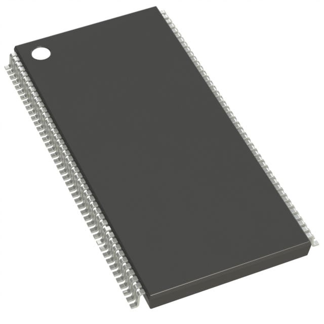
| Device Package | 86-TSOP II | Memory Format | DRAM | Technology | SDRAM | ||
|---|---|---|---|---|---|---|---|
| Memory Size | 256 Mbit | Access Time | 5.5 ns | Grade | Industrial | ||
| Clock Frequency | 143 MHz | Voltage | 3V ~ 3.6V | Memory Type | Volatile | ||
| Operating Temperature | -40°C ~ 85°C (TA) | Write Cycle Time Word Page | N/A | Packaging | 86-TFSOP (0.400", 10.16mm Width) | ||
| Mounting Method | Volatile | Memory Interface | Parallel | Memory Organization | 8M x 32 | ||
| Moisture Sensitivity Level | 3 (168 Hours) | RoHS Compliance | ROHS3 Compliant | REACH Compliance | REACH Unaffected | ||
| Qualification | N/A | ECCN | EAR99 | HTS Code | 8542.32.0024 |
Overview of IS42S32800B-7TLI – IC DRAM 256MBIT PAR 86TSOP II
The IS42S32800B-7TLI is a 256-Mbit synchronous DRAM organized as 8M × 32 with a parallel interface and four internal banks. It implements a fully synchronous, pipelined architecture with programmable burst operation to deliver high memory bandwidth for board-level memory subsystems.
Key electrical and mechanical characteristics include a 3.3V (3.0–3.6V) supply range, a 143 MHz clock frequency option, 5.5 ns access time, and an 86-pin TSOP-II package. The device is specified for an ambient operating range of −40°C to 85°C.
Key Features
- Memory Architecture — 256 Mbit organized as 8M × 32 with four internal banks (2M × 32 × 4), enabling burst and banked access patterns.
- Synchronous SDRAM — Fully synchronous operation with internal pipelined architecture; all inputs sampled on the positive edge of CLK for deterministic timing.
- Clock and Timing — Clock frequency option at 143 MHz and specified access time of 5.5 ns; supports CAS# latency 2 or 3 as programmable in the mode register.
- Burst and Transfer Control — Programmable burst lengths of 1, 2, 4, 8 or full-page with interleaved or linear burst types, plus burst-stop and burst-read-single-write operation.
- Refresh and Low-Power Modes — Auto Refresh and Self Refresh supported; 4096 refresh cycles/64 ms (and 4096/32 ms noted for industrial grade), with power-down and self-refresh modes that disable input buffers to reduce standby power.
- Byte Masking and Data Control — Individual byte control via DQM0–DQM3 for masked write/read operations on the 32-bit data bus.
- Voltage and Interface — Single +3.3V ±0.3V power supply with LVTTL-compatible interface signals.
- Package and Thermal — Available in an 86-pin TSOP-II (0.400", 10.16 mm width) package and specified for −40°C to 85°C ambient operating temperature.
Typical Applications
- High-memory-bandwidth systems — Intended for designs that require sustained SDRAM throughput and burst transfers.
- Board-level DRAM expansion — Acts as a parallel DRAM component for systems needing 256 Mbit density in an 86-pin TSOP-II package.
- Systems requiring controlled refresh — Suitable where Auto Refresh and Self Refresh modes with defined refresh-cycle behavior are required.
Unique Advantages
- Quad-bank architecture: Four internal banks (2M × 32 each) permit concurrent bank operations and efficient burst sequencing for higher effective throughput.
- Programmable timing and bursts: Mode-register programmable CAS latency and selectable burst lengths let designers tune latency and transfer behavior to system needs.
- Byte-level data control: DQM0–DQM3 individual byte masking enables fine-grained write/read control on the 32-bit data bus.
- Synchronous pipelined design: Fully synchronous operation and internal pipelining simplify timing analysis and support deterministic system timing.
- Industrial temperature range: Specified operation from −40°C to 85°C supports deployment in thermally demanding environments.
- Industry-standard supply and I/O: Single +3.3V supply and LVTTL interface compatibility ease integration with common system logic levels.
Why Choose IS42S32800B-7TLI?
The IS42S32800B-7TLI provides a compact 256-Mbit SDRAM solution with a synchronous, pipelined architecture, programmable latency and burst options, and four internal banks to support higher-bandwidth memory operations. Its 3.3V single-supply operation, 32-bit data path, and TSOP-II package make it suitable for board-level memory implementations where predictable timing and refresh control are required.
This device is appropriate for designs that need a deterministic, high-throughput parallel DRAM with selectable timing and power modes. Its specified ambient temperature range and refresh behavior offer flexibility for a range of system environments where reliable DRAM operation is required over standard industrial temperature ranges.
If you would like pricing, availability, or a formal quote for IS42S32800B-7TLI, submit a request and our team will respond with a quote and technical details to support your design evaluation.