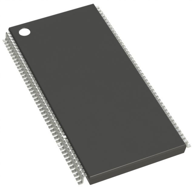
IS42S32800B-7TI
| Part Description |
IC DRAM 256MBIT PAR 86TSOP II |
|---|---|
| Quantity | 104 Available (as of June 15, 2026) |

| Product Category | DRAM Memory |
|---|---|
| Manufacturer | Integrated Silicon Solution Inc |
| Manufacturing Status | Obsolete |
| Manufacturer Standard Lead Time | Contact Us |
| Datasheet |
Specifications & Environmental
| Device Package | 86-TSOP II | Memory Format | DRAM | Technology | SDRAM | ||
|---|---|---|---|---|---|---|---|
| Memory Size | 256 Mbit | Access Time | 5.5 ns | Grade | Industrial | ||
| Clock Frequency | 143 MHz | Voltage | 3V ~ 3.6V | Memory Type | Volatile | ||
| Operating Temperature | -40°C ~ 85°C (TA) | Write Cycle Time Word Page | N/A | Packaging | 86-TFSOP (0.400", 10.16mm Width) | ||
| Mounting Method | Volatile | Memory Interface | Parallel | Memory Organization | 8M x 32 | ||
| Moisture Sensitivity Level | 3 (168 Hours) | RoHS Compliance | ROHS Compliant | REACH Compliance | REACH Unaffected | ||
| Qualification | N/A | ECCN | EAR99 | HTS Code | 8542.32.0024 |
Overview of IS42S32800B-7TI – IC DRAM 256MBIT PAR 86TSOP II
The IS42S32800B-7TI is a 256‑Mbit synchronous DRAM organized as four internal banks of 2M × 32 bits (total 8M × 32). It implements a fully synchronous, pipelined architecture with programmable burst and mode options to support structured, high‑bandwidth memory access patterns.
Designed for systems that require deterministic, high-throughput DRAM, the device supports clock rates of 166/143 MHz, single‑supply operation at 3.3 V ±0.3 V, and an industrial operating range from -40°C to 85°C. The device is available in an 86‑pin TSOP II package (0.400", 10.16 mm width).
Key Features
- Memory Architecture — Quad-bank organization: four internal banks of 2M × 32 bits (total 8M × 32), enabling interleaved accesses and sustained throughput for burst operations.
- Synchronous SDRAM — Fully synchronous operation with internal pipelined architecture; all signals registered on the positive edge of CLK for predictable timing.
- Performance — Supports clock rates of 166/143 MHz and access time of 5.5 ns; CAS latency selectable at 2 or 3 to match system timing requirements.
- Burst and Mode Control — Programmable burst lengths (1, 2, 4, 8 or full page), burst type selectable (interleaved or linear), burst‑read/single‑write and burst stop functions for flexible data transfer patterns.
- Refresh and Power Management — Auto Refresh and Self Refresh supported with 4096 refresh cycles/64 ms (15.6 µs/row) and 4096 cycles/32 ms for industrial grade; CKE provides clock enable control for power-down and self-refresh entry.
- Byte Control and Interface — Individual byte enables via DQM0–DQM3 and LVTTL interface for compatibility with common system logic levels.
- Voltage and Temperature — Single +3.3 V ±0.3 V supply; operating temperature range -40°C to 85°C (TA).
- Package — 86‑pin TSOP‑II (0.50 mm pin pitch, 8 × 13 mm footprint) suitable for compact board layouts; Pb‑free package option available.
Typical Applications
- High‑bandwidth memory subsystems — Suited to systems that require structured burst transfers and sustained throughput due to its quad‑bank, pipelined SDRAM architecture.
- Embedded processors and controllers — Provides synchronous DRAM storage with selectable CAS latency and burst modes for timing‑sensitive embedded designs.
- Networking and communications equipment — Useful where deterministic, high‑speed memory accesses and byte‑level masking (DQM0–3) are required.
Unique Advantages
- Quad‑bank organization: Four internal banks of 2M × 32 bits provide interleaving capability to increase effective memory throughput for burst operations.
- Programmable performance: Selectable CAS latency (2 or 3) and multiple burst lengths allow designers to tune latency and transfer sizes to system requirements.
- Robust refresh options: Auto and Self Refresh modes with specified refresh cycle rates support stable operation across temperature ranges including industrial grade timing.
- Byte‑level control: Individual DQM0–DQM3 byte masking enables partial‑word writes and fine‑grained data handling.
- Industry‑grade voltage and temperature: Single +3.3 V ±0.3 V supply and -40°C to 85°C operating range enable deployment in a wide set of environments.
- Compact package: 86‑pin TSOP‑II package (10.16 mm width) supports dense PCB integration while offering a Pb‑free option.
Why Choose IS42S32800B-7TI?
The IS42S32800B-7TI combines a fully synchronous, pipelined SDRAM core with quad‑bank organization and flexible burst/mode controls to deliver predictable, high‑throughput memory behavior. Its selectable CAS latency, burst options, and byte‑level masking let designers optimize latency and bandwidth tradeoffs for their specific system needs.
This device is appropriate for designers building systems that require deterministic SDRAM performance, industrial temperature operation, and a compact TSOP‑II footprint. Backed by Integrated Silicon Solution, Inc., it provides a specification-driven memory option for applications demanding structured, high‑bandwidth DRAM.
Request a quote or submit an inquiry to obtain pricing and availability for the IS42S32800B-7TI.