IS42S32800D-6B
| Part Description |
IC DRAM 256MBIT PAR 90TFBGA |
|---|---|
| Quantity | 1,819 Available (as of June 15, 2026) |

| Product Category | Memory |
|---|---|
| Manufacturer | Integrated Silicon Solution Inc |
| Manufacturing Status | Obsolete |
| Manufacturer Standard Lead Time | Contact Us |
| Datasheet |
Specifications & Environmental
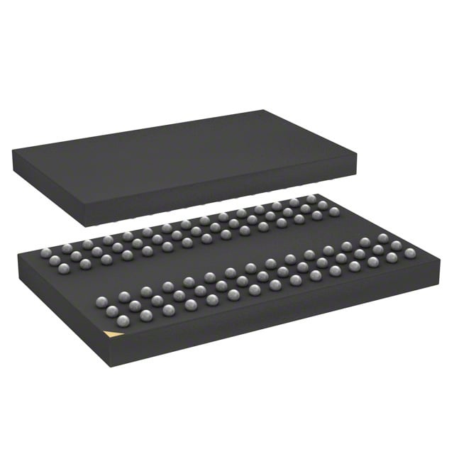
| Device Package | 90-TFBGA (8x13) | Memory Format | DRAM | Technology | SDRAM | ||
|---|---|---|---|---|---|---|---|
| Memory Size | 256 Mbit | Access Time | 5.4 ns | Grade | Commercial | ||
| Clock Frequency | 166 MHz | Voltage | 3V ~ 3.6V | Memory Type | Volatile | ||
| Operating Temperature | 0°C ~ 70°C (TA) | Write Cycle Time Word Page | N/A | Packaging | 90-TFBGA | ||
| Mounting Method | Volatile | Memory Interface | Parallel | Memory Organization | 8M x 32 | ||
| Moisture Sensitivity Level | 3 (168 Hours) | RoHS Compliance | ROHS3 Compliant | REACH Compliance | REACH Unaffected | ||
| Qualification | N/A | ECCN | EAR99 | HTS Code | 8542.32.0024 |
Overview of IS42S32800D-6B – IC DRAM 256MBIT PAR 90TFBGA
The IS42S32800D-6B is a 256Mbit synchronous DRAM organized as 8M × 32 with an internal quad-bank architecture (2M × 32 × 4 banks). It operates from a single 3.3V supply (3.0V–3.6V) and uses a fully synchronous, positive-edge clocked interface to support high-speed burst transfers and random column access every clock cycle.
This device targets 3.3V memory systems that require programmable burst operation, selectable CAS latency, and standard 90-ball TF‑BGA packaging for compact board-level integration.
Key Features
- Memory Organization and Capacity 256 Mbit SDRAM configured as 8M × 32 and internally arranged as 2M × 32 × 4 banks for bank interleaving and parallel access.
- Synchronous Interface Fully synchronous operation with all signals referenced to the rising edge of the clock and LVTTL-compatible inputs/outputs.
- Clock and Timing Supports up to 166 MHz clock frequency (CAS latency = 3) with an access time from clock of 5.4 ns at CL=3 and programmable CAS latency options (2 or 3 clocks).
- Burst and Sequencing Programmable burst lengths (1, 2, 4, 8, full page) and selectable burst sequence (sequential or interleave), plus burst read/write and burst read/single write modes with burst termination options.
- Refresh and Power Modes Auto Refresh and Self Refresh supported; refresh rate options include 4K refresh cycles in 16 ms (A2 grade) or 64 ms (commercial/A1/industrial options noted in datasheet).
- Power Supply Single power supply operation at 3.3V ±0.3V (specified 3.0V–3.6V).
- Package and Mounting Supplied in a 90‑ball TF‑BGA (8 × 13) package for compact, surface-mounted memory implementations.
- Operating Temperature Commercial operating range specified at 0°C to +70°C (TA) for this part.
Typical Applications
- High‑speed memory subsystems For designs requiring synchronous DRAM with programmable burst lengths and bank interleaving to maximize throughput.
- Systems with tight board area The 90‑ball TF‑BGA package enables compact PCB layouts where board space and signal integrity matter.
- Low-latency data buffering With CAS latency options and 166 MHz operation, suited for applications needing deterministic, low-latency access patterns.
Unique Advantages
- Quad‑bank architecture: Enables internal bank interleaving to hide precharge time and sustain higher sustained data rates.
- Programmable burst control: Selectable burst lengths and sequences provide design flexibility for a variety of memory access patterns.
- High clock-rate option: 166 MHz operation (CL=3) with a 5.4 ns access time from clock supports demanding synchronous memory timing.
- Standard 3.3V supply: Single VDD at 3.3V ±0.3V simplifies power rail design in legacy 3.3V systems.
- Compact TF‑BGA package: 90‑ball TF‑BGA (8×13) reduces PCB footprint while providing a robust surface-mount form factor.
- Refresh and power management: Auto Refresh and Self Refresh support help maintain data integrity and reduce power during idle periods.
Why Choose IC DRAM 256MBIT PAR 90TFBGA?
The IS42S32800D-6B provides a verified 256Mbit SDRAM building block for 3.3V systems that require synchronous burst operation, selectable CAS latency, and quad-bank performance. Its combination of 166 MHz clock capability, programmable burst features, and compact 90‑ball TF‑BGA package make it suitable for designs where throughput, timing flexibility, and board-area efficiency are priorities.
This device is appropriate for engineers specifying standard commercial-temperature synchronous DRAM in applications that rely on predictable timing, bank interleaving, and industry-standard LVTTL signaling.
Request a quote or submit a product inquiry for pricing and availability on the IS42S32800D-6B.