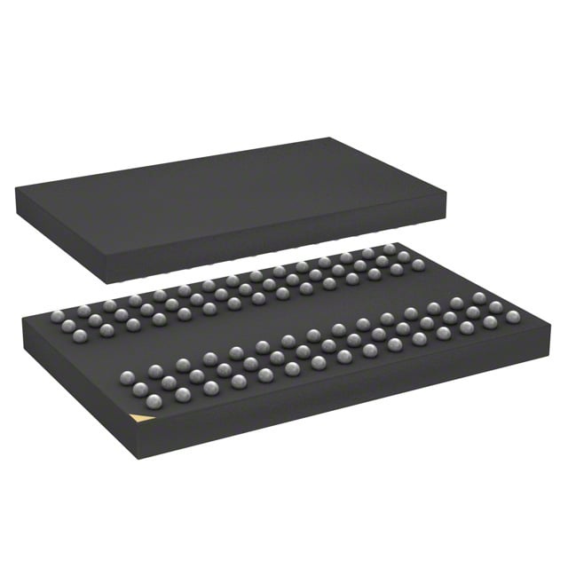
IS42S32800D-6BL
| Part Description |
IC DRAM 256MBIT PAR 90TFBGA |
|---|---|
| Quantity | 640 Available (as of June 8, 2026) |
| Product Category | Memory |
|---|---|
| Manufacturer | Integrated Silicon Solution Inc |
| Manufacturing Status | Obsolete |
| Manufacturer Standard Lead Time | Contact Us |
| Datasheet |
Specifications & Environmental
| Device Package | 90-TFBGA (8x13) | Memory Format | DRAM | Technology | SDRAM | ||
|---|---|---|---|---|---|---|---|
| Memory Size | 256 Mbit | Access Time | 5.4 ns | Grade | Commercial | ||
| Clock Frequency | 166 MHz | Voltage | 3V ~ 3.6V | Memory Type | Volatile | ||
| Operating Temperature | 0°C ~ 70°C (TA) | Write Cycle Time Word Page | N/A | Packaging | 90-TFBGA | ||
| Mounting Method | Volatile | Memory Interface | Parallel | Memory Organization | 8M x 32 | ||
| Moisture Sensitivity Level | 3 (168 Hours) | RoHS Compliance | ROHS3 Compliant | REACH Compliance | REACH Unaffected | ||
| Qualification | N/A | ECCN | EAR99 | HTS Code | 8542.32.0024 |
Overview of IS42S32800D-6BL – IC DRAM 256MBIT PAR 90TFBGA
The IS42S32800D-6BL is a 256Mbit synchronous DRAM organized as 8M × 32 with a parallel interface, designed for 3.3V memory systems. It uses a pipelined, quad-bank architecture with all signals referenced to the rising edge of the system clock.
This device targets designs that require synchronous burst access, automatic refresh capabilities and predictable timing at clock frequencies up to 166 MHz, all delivered in a compact 90‑TFBGA (8×13) package for board-level integration.
Key Features
- Memory Architecture — 256 Mbit SDRAM organized as 8M × 32 with 4 internal banks (2M × 32 × 4 banks) for interleaved access and hidden precharge.
- Performance & Timing — Supports clock frequencies up to 166 MHz (CAS latency options 2 or 3); access time from clock as low as 5.4 ns at CAS‑3.
- Synchronous Interface — Fully synchronous operation with LVTTL-compatible inputs and all signals registered on the positive clock edge.
- Burst and CAS Control — Programmable burst length (1, 2, 4, 8, full page) and burst sequence (sequential/interleave); burst read/write and burst read/single write supported with burst termination commands.
- Refresh and Power Modes — Auto Refresh and Self Refresh supported; refresh counts per datasheet (4K cycles every 16 ms for A2 grade or 64 ms for commercial/other grades).
- Supply and Voltage — Single power supply operation at 3.3 V ±0.3 V (3.0 V to 3.6 V listed); LVTTL signal levels.
- Package and Temperature — Supplied in a 90‑ball TF‑BGA (8×13) package; this commercial variant specifies an operating temperature range of 0°C to +70°C.
Typical Applications
- 3.3V memory subsystems — Provides 256 Mbit of synchronous DRAM for system memory buses requiring parallel SDRAM with programmable burst behavior.
- High-speed buffering — Quad-bank organization and burst modes enable predictable burst transfers and bank interleaving for buffering and data staging.
- Embedded platforms — Compact 90‑TFBGA packaging and LVTTL interface suit board-level integration where a 256Mbit synchronous DRAM is required.
Unique Advantages
- Deterministic synchronous timing: Fully synchronous design with registered inputs and programmable CAS latency provides predictable timing for system designers.
- Flexible burst control: Programmable burst lengths and sequences allow optimization of consecutive reads/writes to match system access patterns.
- Bank interleaving: Four internal banks hide precharge time and enable higher effective throughput during interleaved accesses.
- Industry-standard supply and interface: Operates at 3.3 V (±0.3 V) with LVTTL I/O, simplifying integration into existing 3.3 V memory systems.
- Compact BGA footprint: 90‑TFBGA (8×13) package reduces board area while providing the required pinout for parallel SDRAM operation.
Why Choose IC DRAM 256MBIT PAR 90TFBGA?
The IS42S32800D-6BL delivers a 256Mbit synchronous DRAM option with a pipelined, quad-bank architecture and programmable burst behavior suited to systems that need predictable, high-speed parallel memory. Its timing options (CAS‑2/3), support for auto and self refresh, and LVTTL interface make it a practical choice for 3.3 V memory designs where deterministic access and compact packaging are important.
This commercial-grade part is ideal for engineers and procurement teams specifying on-board SDRAM for embedded platforms and memory subsystems that require a 90‑TFBGA package, documented timing characteristics up to 166 MHz, and standard 3.3 V operation.
Request a quote or submit an inquiry for pricing and availability to evaluate the IS42S32800D-6BL for your design needs.