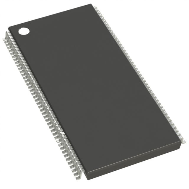
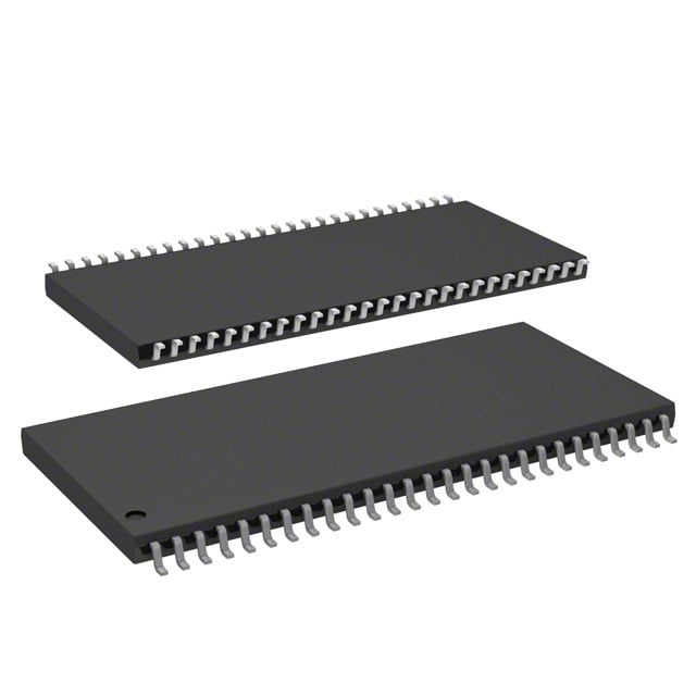
IS42S81600D-6TL
| Part Description |
IC DRAM 128MBIT PAR 54TSOP II |
|---|---|
| Quantity | 314 Available (as of June 15, 2026) |

| Product Category | Memory |
|---|---|
| Manufacturer | Integrated Silicon Solution Inc |
| Manufacturing Status | Obsolete |
| Manufacturer Standard Lead Time | Contact Us |
| Datasheet |
Specifications & Environmental
| Device Package | 54-TSOP II | Memory Format | DRAM | Technology | SDRAM | ||
|---|---|---|---|---|---|---|---|
| Memory Size | 128 Mbit | Access Time | 5.4 ns | Grade | Commercial | ||
| Clock Frequency | 166 MHz | Voltage | 3V ~ 3.6V | Memory Type | Volatile | ||
| Operating Temperature | 0°C ~ 70°C (TA) | Write Cycle Time Word Page | N/A | Packaging | 54-TSOP (0.400", 10.16mm Width) | ||
| Mounting Method | Volatile | Memory Interface | Parallel | Memory Organization | 16M x 8 | ||
| Moisture Sensitivity Level | 3 (168 Hours) | RoHS Compliance | ROHS3 Compliant | REACH Compliance | REACH Unaffected | ||
| Qualification | N/A | ECCN | EAR99 | HTS Code | 8542.32.0002 |
Overview of IS42S81600D-6TL – IC DRAM 128MBIT PAR 54TSOP II
The IS42S81600D-6TL is a 128 Mbit synchronous DRAM (SDRAM) organized as 16M × 8 with a parallel memory interface. It uses a pipeline, fully synchronous architecture with all signals referenced to the rising edge of the system clock for predictable timing and high-speed burst transfers.
This device is intended for designs that require compact board-level SDRAM density with programmable burst control, selectable CAS latency, and built-in refresh modes to manage power and data integrity in active and low-power states.
Key Features
- Core Architecture Fully synchronous SDRAM with pipeline architecture and internal quad-bank organization to enable high-speed burst-oriented transfers and bank interleaving.
- Memory Configuration 128 Mbit capacity organized as 16M × 8 (4 banks of 33,554,432 bits each) to support compact, byte-wide memory implementations.
- Clock and Timing Supports up to 166 MHz clock frequency (device -6 speed grade) with programmable CAS latency options of 2 or 3 clocks; typical access time from clock is 5.4 ns at CAS = 3.
- Burst and Access Control Programmable burst lengths (1, 2, 4, 8, full page) and selectable burst sequence (Sequential/Interleave). Supports burst read/write, burst read/single write, and burst termination via burst stop and auto-precharge.
- Refresh and Power Modes Auto Refresh (CBR) and Self Refresh with programmable refresh periods; 4096 refresh cycles every 64 ms. Includes power-saving power-down and self-refresh capabilities.
- Interface and Signaling LVTTL-compatible inputs/outputs with all signals referenced to CLK for synchronous operation on the rising clock edge.
- Power Operates from a nominal 3.3 V supply; specified supply range 3.0 V to 3.6 V (VDD/VDDQ = 3.3 V per device specification).
- Package and Temperature 54-pin TSOP II package (0.400", 10.16 mm width). Operating ambient temperature specified at 0°C to 70°C (TA).
- Compliance Notes Device features list includes lead-free availability as noted in the product specification set.
Typical Applications
- High-speed buffering — Use for burst-oriented frame or packet buffering where synchronous, clocked transfers and fast access time are required.
- System memory subsystems — Board-level SDRAM expansion for designs that require a 128 Mbit, byte-wide memory component with programmable burst control.
- Low-power standby designs — Systems that benefit from Self Refresh and power-down modes to reduce power during idle periods while retaining data integrity.
Unique Advantages
- Synchronous, clock-referenced operation: All inputs and outputs are registered on the rising edge of CLK, simplifying timing closure in synchronous memory subsystems.
- Flexible burst control: Programmable burst lengths and sequences allow designers to optimize throughput and latency for different access patterns.
- Selectable CAS latency and high clock rate: CAS = 2 or 3 options and a 166 MHz (-6) speed grade enable trade-offs between latency and maximum clock frequency.
- Built-in refresh management: Auto Refresh and Self Refresh with defined refresh cycles (4096/64 ms) simplify retention and power management.
- Compact board footprint: 54-pin TSOP II package (10.16 mm width) provides 128 Mbit density in a small form factor for space-constrained designs.
Why Choose IS42S81600D-6TL?
The IS42S81600D-6TL combines a compact 128 Mbit SDRAM density with fully synchronous, pipeline architecture and flexible burst/CAS options to address designs that need predictable, high-speed memory behavior. Its LVTTL interface, programmable refresh, and power-down/self-refresh modes provide practical control over performance and power in system-level implementations.
This device is well suited for engineers specifying board-level synchronous DRAM where a 16M × 8 organization, 3.3 V operation, selectable CAS latency, and a 54-pin TSOP II package meet the design constraints for timing, space, and power management.
Request a quote or submit a request for pricing and availability to discuss how the IS42S81600D-6TL fits your next design.