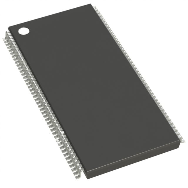
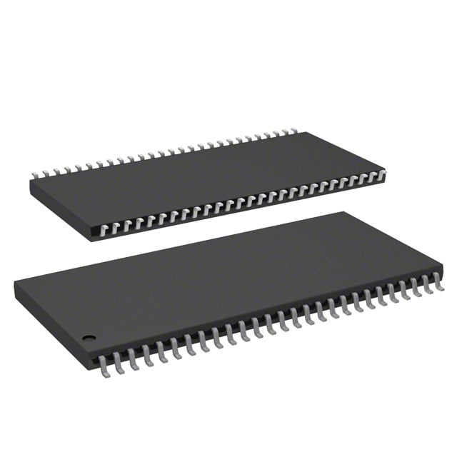
IS42S81600D-7TL
| Part Description |
IC DRAM 128MBIT PAR 54TSOP II |
|---|---|
| Quantity | 517 Available (as of June 17, 2026) |

| Product Category | DRAM Memory |
|---|---|
| Manufacturer | Integrated Silicon Solution Inc |
| Manufacturing Status | Obsolete |
| Manufacturer Standard Lead Time | Contact Us |
| Datasheet |
Specifications & Environmental
| Device Package | 54-TSOP II | Memory Format | DRAM | Technology | SDRAM | ||
|---|---|---|---|---|---|---|---|
| Memory Size | 128 Mbit | Access Time | 5.4 ns | Grade | Commercial | ||
| Clock Frequency | 143 MHz | Voltage | 3V ~ 3.6V | Memory Type | Volatile | ||
| Operating Temperature | 0°C ~ 70°C (TA) | Write Cycle Time Word Page | N/A | Packaging | 54-TSOP (0.400", 10.16mm Width) | ||
| Mounting Method | Volatile | Memory Interface | Parallel | Memory Organization | 16M x 8 | ||
| Moisture Sensitivity Level | 3 (168 Hours) | RoHS Compliance | ROHS Compliant | REACH Compliance | REACH Unaffected | ||
| Qualification | N/A | ECCN | EAR99 | HTS Code | 8542.32.0002 |
Overview of IS42S81600D-7TL – IC DRAM 128MBIT PAR 54TSOP II
The IS42S81600D-7TL is a 128 Mbit synchronous DRAM (SDRAM) organized as 16M × 8 with a parallel memory interface. It implements a quad-bank, fully synchronous architecture with pipeline operation and LVTTL input/output signaling for burst-oriented read/write access.
This device is intended for board-level memory subsystems that require programmable burst operation, selectable CAS latency, and operation from a nominal 3.3 V supply range, delivered in a 54-pin TSOP II package (0.400", 10.16 mm width).
Key Features
- Core / Architecture Fully synchronous SDRAM with internal quad-bank organization and pipeline architecture to support high-speed burst transfers.
- Memory 128 Mbit total capacity organized as 16M × 8; random column address capability every clock cycle and burst read/write operation.
- Performance Specified for a 143 MHz clock frequency (–7 speed grade) with programmable CAS latency (2 or 3 clocks) and an access time from clock of 5.4 ns for CAS latency = 3.
- Burst & Sequencing Programmable burst length (1, 2, 4, 8, full page) and selectable burst sequence (sequential or interleave); supports burst termination and auto-precharge.
- Refresh & Power Modes Auto Refresh and Self Refresh support with 4,096 refresh cycles every 64 ms and available power-down mode.
- Interface & Signaling LVTTL-compatible inputs and outputs; all inputs and outputs are registered to the rising edge of the clock (CLK).
- Supply & Package Operates from 3.0 V to 3.6 V supply range; supplied in a 54-pin TSOP II (0.400", 10.16 mm width) package.
- Manufacturing Options Lead-free availability noted in the device specification.
- Operating Range Specified operating ambient temperature: 0°C to 70°C (TA).
Typical Applications
- Synchronous memory subsystems Use as a 128 Mbit SDRAM device in systems requiring burst-oriented, clock-referenced DRAM.
- Board-level memory modules Fits designs that require a 54-pin TSOP II package and a 3.3 V SDRAM interface with LVTTL signaling.
- Systems needing programmable bursts and CAS latency Applicable where selectable burst lengths, burst sequence, and CAS latency (2 or 3 clocks) are required for timing flexibility.
Unique Advantages
- Quad-bank synchronous architecture Enables interleaving between banks to hide precharge time and maintain continuous burst access.
- High-speed operation (–7 speed grade) Supports 143 MHz clock operation with an access time from clock of 5.4 ns at CAS latency = 3, enabling tight read/write timing.
- Flexible burst control Programmable burst lengths and sequence options (sequential/interleave) allow tailoring transfer behavior to system requirements.
- Comprehensive refresh support Auto Refresh and Self Refresh with 4,096 refresh cycles per 64 ms for maintained data integrity during operation and standby.
- Standard 3.3 V LVTTL interface Simplifies integration into 3.3 V memory systems with LVTTL-compatible signaling.
- Board-level package compatibility 54-pin TSOP II package (10.16 mm width) for direct placement in systems designed for TSOP memory devices.
Why Choose IS42S81600D-7TL?
The IS42S81600D-7TL delivers a compact 128 Mbit SDRAM solution with synchronous, burst-oriented operation, selectable CAS latency, and bank-interleaving to support sustained high-speed transfers. Its 54-pin TSOP II package and LVTTL signaling make it suitable for board-level memory implementations operating from a 3.0 V to 3.6 V supply.
This device is appropriate for designs that require programmable burst control, refresh capability, and predictable timing (143 MHz, CL=3 access time 5.4 ns). Its combination of synchronous pipeline architecture and standard packaging provides a straightforward integration path for systems using parallel SDRAM.
Request a quote or contact sales to obtain pricing, availability, and ordering information for the IS42S81600D-7TL.