IS45S32200E-6BLA1
| Part Description |
IC DRAM 64MBIT PARALLEL 90TFBGA |
|---|---|
| Quantity | 786 Available (as of June 17, 2026) |

| Product Category | DRAM Memory |
|---|---|
| Manufacturer | Integrated Silicon Solution Inc |
| Manufacturing Status | Obsolete |
| Manufacturer Standard Lead Time | Contact Us |
| Datasheet |
Specifications & Environmental
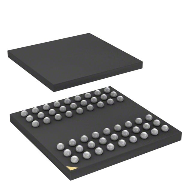
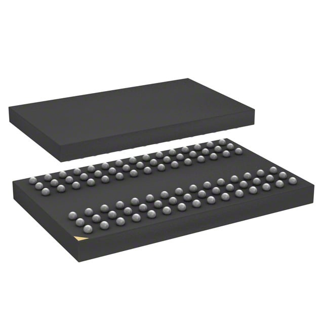
| Device Package | 90-TFBGA (8x13) | Memory Format | DRAM | Technology | SDRAM | ||
|---|---|---|---|---|---|---|---|
| Memory Size | 64 Mbit | Access Time | 5.5 ns | Grade | Industrial | ||
| Clock Frequency | 166 MHz | Voltage | 3V ~ 3.6V | Memory Type | Volatile | ||
| Operating Temperature | -40°C ~ 85°C (TA) | Write Cycle Time Word Page | N/A | Packaging | 90-TFBGA | ||
| Mounting Method | Volatile | Memory Interface | Parallel | Memory Organization | 2M x 32 | ||
| Moisture Sensitivity Level | 3 (168 Hours) | RoHS Compliance | ROHS3 Compliant | REACH Compliance | REACH Unaffected | ||
| Qualification | N/A | ECCN | EAR99 | HTS Code | 8542.32.0002 |
Overview of IS45S32200E-6BLA1 – IC DRAM 64MBIT PARALLEL 90TFBGA
The IS45S32200E-6BLA1 is a 64‑Mbit synchronous DRAM (SDRAM) in a 90‑TFBGA (8×13) package, organized as 524,288 × 32 × 4 to provide quad‑bank memory for high‑speed, pipelined operation. It is designed for 3.3 V memory systems with LVTTL signaling and synchronous, clock‑edge referenced control.
This device targets designs that require parallel SDRAM with programmable burst capability, selectable CAS latency, and extended operating temperature support down to −40 °C up to +85 °C.
Key Features
- Core / Architecture Quad‑bank synchronous DRAM organized as 524,288 × 32 × 4 (64 Mbit) with pipeline architecture and internal bank management to hide row access/precharge.
- Memory Organization 2M × 32 memory organization reported as 524,288 × 32 per bank × 4 banks, delivering 67,108,864 bits total capacity.
- Performance & Timing Supports a clock frequency option of 166 MHz for the –6 speed grade and programmable CAS latency of 2 or 3 clocks; typical access time from clock is 5.5 ns at CL = 3 for the –6 device.
- Burst & Sequencing Programmable burst length (1, 2, 4, 8, full page) and selectable burst sequence (sequential/interleave) for flexible read/write burst operations.
- Refresh & Self‑Refresh Supports AUTO REFRESH and self‑refresh modes with device refresh specifications listed in the datasheet (4096 refresh cycles per refresh period options per grade).
- Power & Interface Single 3.3 V power supply operation (3.0 V to 3.6 V range specified) with LVTTL compatible interface signaling.
- Package & Temperature Range 90‑ball TF‑BGA (8×13) package; operating temperature range specified as −40 °C to +85 °C (TA).
Typical Applications
- Parallel memory subsystems Serves as board‑level SDRAM for systems requiring 64 Mbit of parallel synchronous memory at 3.3 V.
- High‑speed buffering Useful for buffering and burst data transfers where programmable burst lengths and selectable CAS latency improve timing flexibility.
- Embedded and industrial platforms Appropriate for designs that need operation across −40 °C to +85 °C and standard LVTTL interfacing.
Unique Advantages
- Quad‑bank architecture: Internal bank structure enables overlapping commands and improved throughput in pipelined access patterns.
- Configurable burst operation: Multiple burst lengths and sequence modes allow designers to match memory transfers to system data patterns and bus timing.
- Selectable CAS latency: CAS latency options (2 or 3) provide a tradeoff between clock rate and access timing to fit system performance targets.
- Standard 3.3 V supply and LVTTL interface: Simplifies integration into legacy 3.3 V memory systems and supports common logic level interfaces.
- Compact TF‑BGA footprint: The 90‑ball TFBGA (8×13) package offers a compact solution for board designs with limited PCB area.
- Extended operating temperature: Specified −40 °C to +85 °C operation supports a wide range of ambient conditions for industrial applications.
Why Choose IS45S32200E-6BLA1?
The IS45S32200E-6BLA1 provides a straightforward 64‑Mbit synchronous DRAM solution for systems requiring parallel SDRAM with programmable burst modes, selectable CAS latency, and quad‑bank operation. Its 3.3 V single‑supply LVTTL interface and 90‑TFBGA package make it suitable for compact board‑level memory implementations where predictable timing and pipelined operation are required.
Designers targeting embedded or industrial platforms that need documented timing parameters (including access time, clock frequency options, and refresh modes) will find the IS45S32200E-6BLA1 aligned to those needs, offering verifiable specifications for integration and long‑term use.
Request a quote or submit an RFQ to get pricing and availability information for the IS45S32200E-6BLA1 and to receive technical support or procurement details.