IS45S32200E-6TLA1
| Part Description |
IC DRAM 64MBIT PAR 86TSOP II |
|---|---|
| Quantity | 676 Available (as of June 10, 2026) |

| Product Category | Memory |
|---|---|
| Manufacturer | Integrated Silicon Solution Inc |
| Manufacturing Status | Obsolete |
| Manufacturer Standard Lead Time | Contact Us |
| Datasheet |
Specifications & Environmental
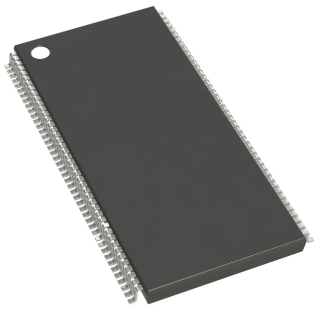
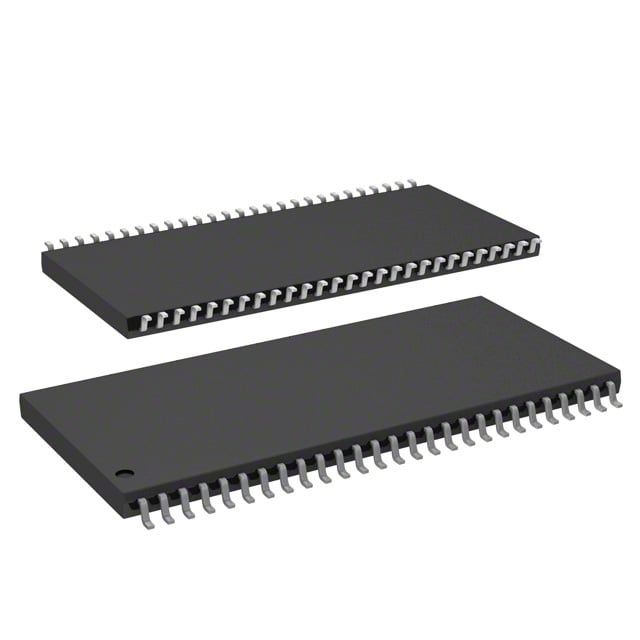
| Device Package | 86-TSOP II | Memory Format | DRAM | Technology | SDRAM | ||
|---|---|---|---|---|---|---|---|
| Memory Size | 64 Mbit | Access Time | 5.5 ns | Grade | Industrial | ||
| Clock Frequency | 166 MHz | Voltage | 3V ~ 3.6V | Memory Type | Volatile | ||
| Operating Temperature | -40°C ~ 85°C (TA) | Write Cycle Time Word Page | N/A | Packaging | 86-TFSOP (0.400", 10.16mm Width) | ||
| Mounting Method | Volatile | Memory Interface | Parallel | Memory Organization | 2M x 32 | ||
| Moisture Sensitivity Level | 3 (168 Hours) | RoHS Compliance | ROHS3 Compliant | REACH Compliance | REACH Unaffected | ||
| Qualification | N/A | ECCN | EAR99 | HTS Code | 8542.32.0002 |
Overview of IS45S32200E-6TLA1 – IC DRAM 64MBIT PAR 86TSOP II
The IS45S32200E-6TLA1 is a 64‑Mbit synchronous DRAM device from Integrated Silicon Solution, Inc. It is organized as 2M × 32 with four internal banks and a fully synchronous, pipeline architecture for high‑speed data transfer in 3.3 V memory systems.
This device targets designs that require parallel SDRAM with programmable burst and latency options, offering deterministic timing and internal bank management to improve effective access performance.
Key Features
- Memory Capacity & Organization 64 Mbit total capacity, organized as 2M × 32 with 4 internal banks; each bank is configured as 2,048 rows × 256 columns × 32 bits.
- Synchronous SDRAM Architecture Fully synchronous design with all signals referenced to a positive clock edge and pipeline architecture for high‑speed transfers.
- Clock & Timing Device variant supports a 166 MHz clock frequency with an access time from clock of 5.5 ns (CAS‑latency = 3) and programmable CAS latency options (2 or 3 clocks).
- Burst & Access Control Programmable burst lengths (1, 2, 4, 8, full page) and sequential/interleave burst sequences; supports burst read/write and burst read/single write operations and burst termination commands.
- Refresh & Self‑Refresh Supports AUTO REFRESH and self‑refresh modes with device refresh cycle specifications provided in the datasheet (4096 refresh cycles per 16 ms or 64 ms depending on grade).
- Interface & Signaling LVTTL compatible interface with parallel memory signaling for system integration.
- Power Single 3.3 V supply operation with a specified supply range of 3.0 V to 3.6 V.
- Package & Temperature Available in an 86‑pin TSOP‑II package (86‑TFSOP, 0.400" / 10.16 mm width) and specified operating temperature range of −40 °C to +85 °C (TA) for industrial use.
Typical Applications
- Embedded memory systems — Provides 64 Mbit of synchronous DRAM for 3.3 V system memory needs where deterministic, clocked operation is required.
- Board‑level memory expansion — Parallel SDRAM organization and TSOP‑II packaging enable integration on system boards for added DRAM capacity.
- Industrial equipment — Specified −40 °C to +85 °C operating range supports deployment in industrial temperature environments.
- Designs requiring programmable timing — Programmable CAS latency and burst control allow tuning of access behavior for system timing requirements.
Unique Advantages
- Quad‑bank architecture: Internal 4‑bank organization hides row access/precharge to improve effective throughput for burst operations.
- Flexible burst and latency control: Programmable burst lengths and CAS latency (2 or 3 clocks) let designers match device behavior to system timing and throughput needs.
- Deterministic synchronous interface: Fully synchronous operation with LVTTL signaling provides predictable timing referenced to the positive clock edge.
- Single 3.3 V supply: Standard 3.3 V operation (3.0 V–3.6 V range) simplifies power rail requirements in common memory subsystems.
- Industrial temperature rating: −40 °C to +85 °C operating range supports use in temperature‑sensitive industrial applications.
- Compact TSOP‑II package: 86‑pin TSOP‑II (10.16 mm width) enables dense board placement while providing parallel DRAM connectivity.
Why Choose IC DRAM 64MBIT PAR 86TSOP II?
The IS45S32200E-6TLA1 delivers a practical combination of 64 Mbit capacity, synchronous pipeline architecture, and programmable burst/latency controls for systems that require predictable, clocked DRAM behavior at 166 MHz. Its 2M × 32 organization and four internal banks make it suitable for designs that need efficient burst access and bank interleaving.
Manufactured by Integrated Silicon Solution, Inc., this device is specified for 3.3 V systems and an industrial temperature range, making it appropriate for embedded and board‑level memory expansion where compact TSOP‑II packaging and configurable timing are required.
Request a quote or submit a request for pricing and availability to discuss integration details and lead times for the IS45S32200E-6TLA1.