IS45S32200E-7BLA2
| Part Description |
IC DRAM 64MBIT PAR 90TFBGA |
|---|---|
| Quantity | 997 Available (as of June 14, 2026) |

| Product Category | Memory |
|---|---|
| Manufacturer | Integrated Silicon Solution Inc |
| Manufacturing Status | Obsolete |
| Manufacturer Standard Lead Time | Contact Us |
| Datasheet |
Specifications & Environmental
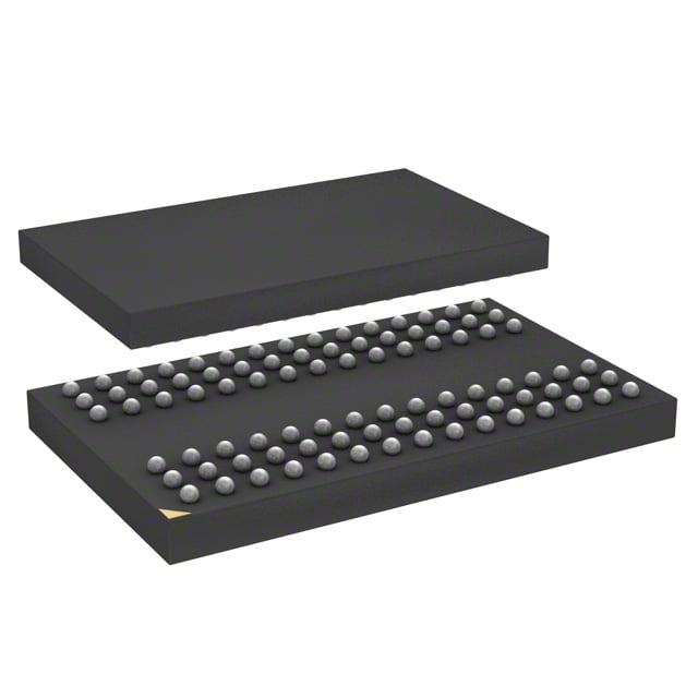
| Device Package | 90-TFBGA (8x13) | Memory Format | DRAM | Technology | SDRAM | ||
|---|---|---|---|---|---|---|---|
| Memory Size | 64 Mbit | Access Time | 5.5 ns | Grade | Automotive | ||
| Clock Frequency | 143 MHz | Voltage | 3V ~ 3.6V | Memory Type | Volatile | ||
| Operating Temperature | -40°C ~ 105°C (TA) | Write Cycle Time Word Page | N/A | Packaging | 90-TFBGA | ||
| Mounting Method | Volatile | Memory Interface | Parallel | Memory Organization | 2M x 32 | ||
| Moisture Sensitivity Level | 3 (168 Hours) | RoHS Compliance | ROHS3 Compliant | REACH Compliance | REACH Unaffected | ||
| Qualification | N/A | ECCN | EAR99 | HTS Code | 8542.32.0002 |
Overview of IS45S32200E-7BLA2 – IC DRAM 64MBIT PAR 90TFBGA
The IS45S32200E-7BLA2 is a 64 Mbit synchronous DRAM (SDRAM) device organized as 2M × 32 with a quad-bank architecture and pipeline operation. It is designed for 3.3 V memory systems and provides a parallel LVTTL interface for high-speed, clocked data transfers.
This -7 timing grade supports up to 143 MHz clock operation with an access time of 5.5 ns and offers programmable burst and CAS timing for flexible memory subsystem integration across temperature ranges down to -40°C and up to 105°C (TA).
Key Features
- Core & Architecture Quad-bank synchronous DRAM with pipeline architecture; all inputs and outputs are referenced to the rising clock edge for deterministic timing.
- Memory Organization & Capacity 64 Mbit total capacity, internally configured as 524,288 × 32 × 4 banks (each bank 16,777,216 bits) organized as 2,048 rows × 256 columns × 32 bits.
- Performance & Timing -7 timing grade supports 143 MHz clock frequency and 5.5 ns access time. Programmable CAS latency (2 or 3 clocks) and programmable burst lengths (1, 2, 4, 8, full page) enable matched system timing.
- Interface & Command Support Parallel LVTTL interface with support for sequential/interleave burst sequences, random column address every clock cycle, burst read/write and burst read/single write operations, and burst termination commands.
- Power Single-supply operation at 3.3 V with allowable supply range 3.0 V to 3.6 V.
- Refresh & Low-Power Modes Auto refresh and self-refresh modes supported; refresh interval options include 4096 cycles per 16 ms (A2 grade) or 64 ms for other grades as specified.
- Package & Thermal 90-ball TF-BGA (8 × 13) package; operating temperature range specified as -40°C to 105°C (TA) for the listed part configuration.
Typical Applications
- 3.3 V Memory Systems Designed for board-level memory subsystems that require synchronous DRAM operating at 3.3 V.
- High-Speed Data Transfer Pipeline architecture and up to 143 MHz clocking support high-rate burst transfers and buffering on memory buses.
- Board-Level DRAM Arrays Compact 90-TFBGA package and parallel interface make the device suitable for dense memory arrays on printed circuit boards.
- Systems Requiring Flexible Timing Programmable CAS latency and burst sequencing enable tuning for a range of system timing requirements.
Unique Advantages
- Predictable Synchronous Timing: Fully synchronous operation referenced to the clock rising edge and programmable CAS latency provide deterministic timing for system designers.
- Flexible Burst Control: Programmable burst lengths and sequence modes (sequential/interleave) simplify burst data transfer matching to host controllers.
- Quad-Bank Architecture: Internal banking with hidden row access/precharge improves effective throughput for interleaved accesses.
- Wide Supply Range: Single-supply operation across 3.0 V to 3.6 V accommodates typical 3.3 V system rails.
- Temperature Range Options: Specified operation from -40°C to 105°C (TA) for the listed configuration supports designs targeting extended temperature environments.
- Compact BGA Footprint: 90-TFBGA (8×13) package enables higher board density and standard surface-mount assembly.
Why Choose IS45S32200E-7BLA2?
The IS45S32200E-7BLA2 delivers a balanced combination of synchronous performance, flexible timing control and a compact package for 64 Mbit DRAM requirements. Its programmable CAS latency, burst modes and quad-bank architecture make it suitable for system designs that need predictable, high-rate burst transfers and configurable access patterns.
This device is appropriate for engineers specifying 3.3 V SDRAM in board-level memory subsystems where controlled timing, refresh options and a small BGA footprint are required. The available operating temperature range and refresh-mode options provide configurability for a range of deployment environments.
Request a quote or submit a specification inquiry to obtain pricing and availability information for the IS45S32200E-7BLA2.