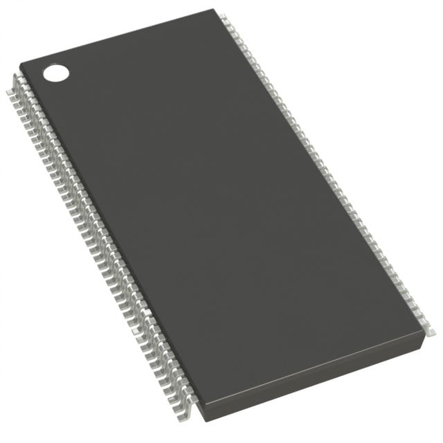
IS45S32200E-7TLA2
| Part Description |
IC DRAM 64MBIT PAR 86TSOP II |
|---|---|
| Quantity | 1,086 Available (as of June 18, 2026) |

| Product Category | DRAM Memory |
|---|---|
| Manufacturer | Integrated Silicon Solution Inc |
| Manufacturing Status | Obsolete |
| Manufacturer Standard Lead Time | Contact Us |
| Datasheet |
Specifications & Environmental
| Device Package | 86-TSOP II | Memory Format | DRAM | Technology | SDRAM | ||
|---|---|---|---|---|---|---|---|
| Memory Size | 64 Mbit | Access Time | 5.5 ns | Grade | Automotive | ||
| Clock Frequency | 143 MHz | Voltage | 3V ~ 3.6V | Memory Type | Volatile | ||
| Operating Temperature | -40°C ~ 105°C (TA) | Write Cycle Time Word Page | N/A | Packaging | 86-TFSOP (0.400", 10.16mm Width) | ||
| Mounting Method | Volatile | Memory Interface | Parallel | Memory Organization | 2M x 32 | ||
| Moisture Sensitivity Level | 3 (168 Hours) | RoHS Compliance | ROHS3 Compliant | REACH Compliance | REACH Unaffected | ||
| Qualification | N/A | ECCN | EAR99 | HTS Code | 8542.32.0002 |
Overview of IS45S32200E-7TLA2 – IC DRAM 64Mbit PAR 86TSOP II
The IS45S32200E-7TLA2 is a 64Mbit synchronous DRAM organized as 524,288 × 32 × 4 banks (64Mb). It implements a fully synchronous pipeline architecture with internal banking to optimize row access and precharge operations.
Designed for 3.3V memory systems requiring a parallel SDRAM interface, this device targets applications that need deterministic clocked access, programmable burst control, and operation across an extended temperature range.
Key Features
- Core / Architecture Quad-bank synchronous DRAM architecture with internal bank management to hide row access/precharge and pipeline data transfer referenced to the rising clock edge.
- Memory Organization & Size 64 Mbit total capacity organized as 2M × 32 per bank (524,288 × 32 × 4 banks).
- Performance -7 speed grade supporting a 143 MHz clock frequency with an access time from clock of 5.5 ns (CAS latency = 3). Multiple clock grades are available (200, 166, 143, 133 MHz in datasheet options).
- Programmable Burst & Latency Programmable burst lengths (1, 2, 4, 8, full page) and burst sequences (sequential/interleave); selectable CAS latency of 2 or 3 clocks.
- Refresh & Self-Refresh Supports auto refresh and self-refresh modes; refresh cycles specified as 4096 every 16 ms for A2 grade or 4096 every 64 ms for other grades per datasheet options.
- Interface & Logic Levels Parallel memory interface with LVTTL-compatible signaling referenced to the positive clock edge.
- Power Single supply operation: 3.0 V to 3.6 V.
- Package & Mounting 86‑pin TSOP‑II (86‑TFSOP, 0.400" / 10.16 mm width) surface-mount package.
- Operating Temperature Rated for operation from −40 °C to +105 °C (TA) as specified for the part variant.
Typical Applications
- 3.3V System Memory: Use as system DRAM in 3.3V designs requiring a 64Mbit parallel SDRAM component with synchronous access.
- High-speed Buffering: Employed where clocked, burstable data transfers are required and predictable CAS-latency timing is needed.
- Industrial Temperature Designs: Suitable for systems that must operate across an extended ambient temperature range (−40 °C to +105 °C TA).
Unique Advantages
- Synchronous, pipelined architecture: All signals referenced to the rising clock edge for deterministic timing and predictable system integration.
- Flexible burst and latency control: Programmable burst lengths and sequences plus selectable CAS latencies (2 or 3 clocks) allow tuning for throughput and latency trade-offs.
- Single 3.3V supply: Simplifies power rail requirements in standard 3.3V memory systems (operates 3.0 V to 3.6 V).
- Extended temperature capability: Specified operation from −40 °C to +105 °C TA for use in temperature-challenging environments.
- Compact TSOP-II package: 86‑pin TSOP‑II footprint (10.16 mm width) enables dense PCB layouts while providing the required pinout for a parallel SDRAM interface.
- Multiple speed-grade options: Datasheet options include 200/166/143/133 MHz grades to match application timing requirements; the -7 grade supports 143 MHz operation.
Why Choose IS45S32200E-7TLA2?
The IS45S32200E-7TLA2 combines a quad-bank synchronous DRAM architecture with programmable burst control and selectable CAS latency to support a range of throughput and latency requirements in 3.3V systems. Its pipeline design and LVTTL interface provide deterministic, clocked operation suitable for designs that rely on predictable memory timing.
This device is appropriate for engineers specifying 64Mbit parallel SDRAM in systems that require flexible burst behavior, a compact TSOP‑II package, and extended ambient temperature operation. The combination of supply range, timing options, and refresh modes offers design flexibility for long-term deployment in temperature-challenging environments.
Request a quote or submit an inquiry to receive pricing and availability information for the IS45S32200E-7TLA2.