IS45S32200E-7TLA2-TR
| Part Description |
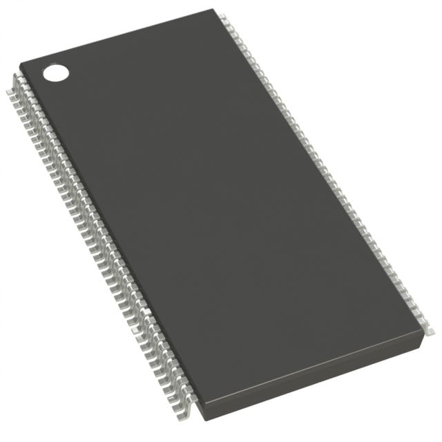
IC DRAM 64MBIT PAR 86TSOP II |
|---|---|
| Quantity | 545 Available (as of June 14, 2026) |

| Product Category | Memory |
|---|---|
| Manufacturer | Integrated Silicon Solution Inc |
| Manufacturing Status | Obsolete |
| Manufacturer Standard Lead Time | Contact Us |
| Datasheet |
Specifications & Environmental
| Device Package | 86-TSOP II | Memory Format | DRAM | Technology | SDRAM | ||
|---|---|---|---|---|---|---|---|
| Memory Size | 64 Mbit | Access Time | 5.5 ns | Grade | Automotive | ||
| Clock Frequency | 143 MHz | Voltage | 3V ~ 3.6V | Memory Type | Volatile | ||
| Operating Temperature | -40°C ~ 105°C (TA) | Write Cycle Time Word Page | N/A | Packaging | 86-TFSOP (0.400", 10.16mm Width) | ||
| Mounting Method | Volatile | Memory Interface | Parallel | Memory Organization | 2M x 32 | ||
| Moisture Sensitivity Level | 3 (168 Hours) | RoHS Compliance | ROHS Compliant | REACH Compliance | REACH Unaffected | ||
| Qualification | N/A | ECCN | EAR99 | HTS Code | 8542.32.0002 |
Overview of IS45S32200E-7TLA2-TR – IC DRAM 64MBIT PAR 86TSOP II
The IS45S32200E-7TLA2-TR is a 64‑Mbit synchronous DRAM (SDRAM) device organized with quad-bank architecture for pipelined, high-speed data transfer. It implements a parallel, LVTTL-compatible interface and is designed for 3.3 V memory systems requiring a 32-bit data path.
This part provides programmable burst operation, selectable CAS latency, and self-refresh capabilities, plus an extended operating temperature option, making it suitable for systems that need deterministic synchronous memory behavior and configurable timing.
Key Features
- Core / Architecture 512K × 32 bits × 4 banks (64‑Mbit) synchronous DRAM with internal bank architecture to hide row access and precharge operations.
- Memory Organization Organized as quad-bank memory with a 32‑bit data width; supports burst read/write and burst read/single write operations.
- Timing & Performance Designed for clock frequencies including 200, 166, 143 and 133 MHz; this -7 variant is specified for 143 MHz with an access time from clock reported at 5.5 ns (CAS latency = 3).
- Programmable Burst & CAS Programmable burst lengths (1, 2, 4, 8, full page) and burst sequence (sequential/interleave); programmable CAS latency options of 2 or 3 clocks.
- Power Single 3.3 V supply operation with specified voltage supply range 3.0 V to 3.6 V.
- Refresh & Self‑Refresh Supports self‑refresh modes; refresh options include 4096 refresh cycles per 16 ms for A2 grade or 64 ms for commercial, industrial and A1 grade options as documented.
- Interface Parallel memory interface with LVTTL input/output signaling referenced to the positive clock edge for synchronous operation.
- Package & Temperature Range Available in 86‑pin TSOP‑II package (0.400", 10.16 mm width); operating temperature range listed as −40°C to +105°C (TA) for the specified grade.
Typical Applications
- 3.3 V memory systems Used as synchronous DRAM in systems that operate from a 3.3 V supply and require a parallel 32‑bit memory interface.
- High‑throughput buffering Suitable for designs needing pipelined, burstable memory transfers with programmable burst length and CAS timing.
- Thermally demanding environments Applicable where extended ambient temperature operation (−40°C to +105°C TA) is required for the memory component.
- Deterministic synchronous control Fits systems that depend on clock‑referenced signaling and predictable access timing (synchronous interface, fixed clock edge operation).
Unique Advantages
- Flexible timing configuration: Programmable CAS latency and burst lengths let designers tune latency and throughput to match system timing requirements.
- Quad‑bank architecture: Internal banking hides row access/precharge, improving effective throughput for interleaved access patterns.
- Broad frequency support: Documented operation at multiple clock rates (200 / 166 / 143 / 133 MHz) with the -7 option specified at 143 MHz, enabling selection of the appropriate speed grade.
- Self‑refresh capability: On‑chip self‑refresh modes and documented refresh cycle options simplify low‑power retention strategies and system refresh management.
- Robust supply range: Operates across a 3.0 V to 3.6 V supply window for tolerance to supply variation within 3.3 V system designs.
- Compact TSOP‑II package: 86‑pin TSOP‑II footprint (10.16 mm width) supports dense board-level memory implementations.
Why Choose IS45S32200E-7TLA2-TR?
The IS45S32200E-7TLA2-TR positions itself as a configurable 64‑Mbit SDRAM solution for designers who need synchronous, burstable memory with selectable timing and banked architecture. Its single 3.3 V supply, LVTTL interface, and documented timing options provide predictable behavior for systems that demand clock‑synchronous data transfers.
This device is appropriate for designs that require a 32‑bit parallel memory interface, programmable burst and CAS settings, and an option for extended ambient temperature operation. Detailed datasheet specifications and multiple speed grades support informed selection and system integration.
Request a quote or submit a product inquiry to receive pricing and availability information for the IS45S32200E-7TLA2-TR.