IS45S32200E-7TLA1
| Part Description |
IC DRAM 64MBIT PAR 86TSOP II |
|---|---|
| Quantity | 468 Available (as of June 14, 2026) |
| Product Category | Memory |
|---|---|
| Manufacturer | Integrated Silicon Solution Inc |
| Manufacturing Status | Obsolete |
| Manufacturer Standard Lead Time | Contact Us |
| Datasheet |
Specifications & Environmental
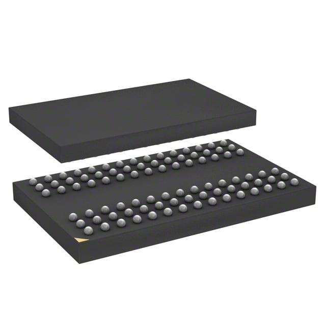
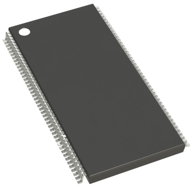
| Device Package | 86-TSOP II | Memory Format | DRAM | Technology | SDRAM | ||
|---|---|---|---|---|---|---|---|
| Memory Size | 64 Mbit | Access Time | 5.5 ns | Grade | Industrial | ||
| Clock Frequency | 143 MHz | Voltage | 3V ~ 3.6V | Memory Type | Volatile | ||
| Operating Temperature | -40°C ~ 85°C (TA) | Write Cycle Time Word Page | N/A | Packaging | 86-TFSOP (0.400", 10.16mm Width) | ||
| Mounting Method | Volatile | Memory Interface | Parallel | Memory Organization | 2M x 32 | ||
| Moisture Sensitivity Level | 3 (168 Hours) | RoHS Compliance | ROHS Compliant | REACH Compliance | REACH Unaffected | ||
| Qualification | N/A | ECCN | EAR99 | HTS Code | 8542.32.0002 |
Overview of IS45S32200E-7TLA1 – IC DRAM 64MBIT PAR 86TSOP II
The IS45S32200E-7TLA1 is a 64‑Mbit synchronous DRAM (SDRAM) organized internally as 524,288 × 32 bits × 4 banks, delivering high‑speed, pipelined memory access for systems that require parallel DRAM. It implements a fully synchronous interface with programmable burst operation and LVTTL signaling.
Designed for 3.3V memory systems, this device targets applications that need a compact TSOP‑II footprint and industrial temperature capability, while providing flexible timing and refresh options to match system performance and power requirements.
Key Features
- Core Architecture Quad‑bank SDRAM organization (524,288 × 32 × 4 banks) with pipelined operation for high throughput and bank interleaving to hide row access/precharge.
- High‑speed Operation Rated for up to 143 MHz clock frequency (‑7 speed grade) with programmable CAS latency options (2 or 3 clocks) and access time as low as 5.5 ns.
- Flexible Burst and Access Modes Programmable burst length (1, 2, 4, 8, full page) and burst sequence (sequential/interleave); supports burst read/write and burst read/single write operations with burst termination commands.
- Power and Interface Single 3.3 V power supply (3.0 V to 3.6 V) with LVTTL interface for command and control signals.
- Refresh and Reliability Supports AUTO REFRESH and self‑refresh modes; provides required refresh cycles per datasheet options (e.g., 4096 refresh cycles over specified intervals depending on grade).
- Package and Temperature Available in an 86‑pin TSOP‑II package (0.400", 10.16 mm width) and specified operating temperature range of −40 °C to +85 °C (TA).
Typical Applications
- Embedded Systems Use as main or buffer DRAM in embedded designs that require a 64‑Mbit SDRAM in a compact 86‑TSOP‑II package operating at 3.3 V.
- Industrial Control Suited for industrial temperature systems (−40 °C to +85 °C TA) where synchronous, banked memory and self‑refresh are required.
- Consumer and Networking Devices Provides parallel SDRAM storage for mid‑range consumer or networking products needing programmable burst modes and LVTTL interfaces.
- Memory Expansion Modules Fits designs that require 64‑Mbit density in TSOP‑II form factor for board‑level memory expansion and system upgrades.
Unique Advantages
- Quad‑bank Architecture: Four internal banks enable hidden row access/precharge to improve effective throughput for interleaved access patterns.
- Programmable Timing: CAS latency selectable (2 or 3 clocks) and multiple burst lengths allow designers to trade latency and throughput to match system timing.
- Compact TSOP‑II Packaging: 86‑pin TSOP‑II (0.400", 10.16 mm width) provides a small footprint for dense board layouts while retaining full SDRAM functionality.
- Industrial Temperature Range: Specified operation from −40 °C to +85 °C (TA) supports deployment in temperature‑sensitive environments.
- Single 3.3 V Supply with LVTTL Interface: Standard 3.3 V power and LVTTL signaling simplify integration into existing 3.3 V memory subsystems.
- Self‑Refresh and Flexible Refresh Options: Built‑in self‑refresh and programmable refresh behavior support low‑power retention and reliable long‑term operation.
Why Choose IS45S32200E-7TLA1?
The IS45S32200E-7TLA1 combines a quad‑bank SDRAM architecture with selectable timing and burst modes to provide a flexible 64‑Mbit memory solution for 3.3 V systems. Its industrial temperature rating and compact 86‑TSOP‑II package make it suitable for embedded, industrial control, and mid‑range consumer/networking designs that require predictable synchronous DRAM behavior.
This device is appropriate for engineers seeking a verifiable, specification‑driven DRAM component offering programmable latency and burst control, banked operation for improved throughput, and standard LVTTL interfacing for straightforward system integration.
Request a quote or submit a sales inquiry to receive pricing and availability information for the IS45S32200E-7TLA1.