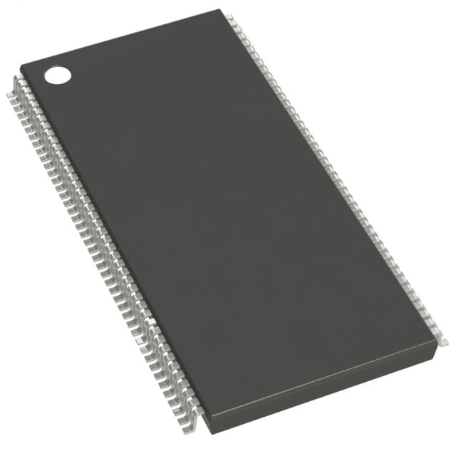
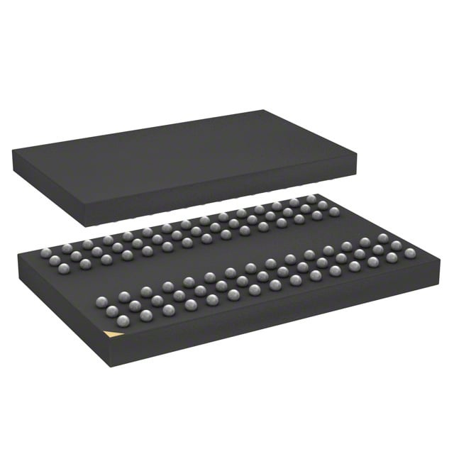
IS45S32200E-7BLA1
| Part Description |
IC DRAM 64MBIT PAR 90TFBGA |
|---|---|
| Quantity | 140 Available (as of June 14, 2026) |

| Product Category | Memory |
|---|---|
| Manufacturer | Integrated Silicon Solution Inc |
| Manufacturing Status | Obsolete |
| Manufacturer Standard Lead Time | Contact Us |
| Datasheet |
Specifications & Environmental
| Device Package | 90-TFBGA (8x13) | Memory Format | DRAM | Technology | SDRAM | ||
|---|---|---|---|---|---|---|---|
| Memory Size | 64 Mbit | Access Time | 5.5 ns | Grade | Industrial | ||
| Clock Frequency | 143 MHz | Voltage | 3V ~ 3.6V | Memory Type | Volatile | ||
| Operating Temperature | -40°C ~ 85°C (TA) | Write Cycle Time Word Page | N/A | Packaging | 90-TFBGA | ||
| Mounting Method | Volatile | Memory Interface | Parallel | Memory Organization | 2M x 32 | ||
| Moisture Sensitivity Level | 3 (168 Hours) | RoHS Compliance | ROHS3 Compliant | REACH Compliance | REACH Unaffected | ||
| Qualification | N/A | ECCN | EAR99 | HTS Code | 8542.32.0002 |
Overview of IS45S32200E-7BLA1 – 64Mbit Parallel SDRAM (90‑TFBGA)
The IS45S32200E-7BLA1 is a 64‑Mbit synchronous dynamic RAM (SDRAM) organized as 524,288 × 32 × 4 banks, delivering a parallel memory interface in a 90‑ball TF‑BGA package. It operates from a single 3.3 V supply and implements a fully synchronous, pipelined architecture with internal banking for improved access efficiency.
This device targets systems requiring compact, low-latency parallel SDRAM with selectable burst behavior and programmable CAS latency. Typical uses include embedded memory subsystems where a 64‑Mbit SDRAM with industrial temperature range and standard LVTTL signaling is required.
Key Features
- Memory organization — 64‑Mbit SDRAM arranged as 524,288 × 32 × 4 banks to support simultaneous bank operation and improved throughput.
- Performance options — Clock frequency options include 200, 166, 143 and 133 MHz; the -7 variant is specified at 143 MHz with an access time of 5.5 ns (CAS‑3).
- Programmable burst and latency — Programmable burst lengths (1, 2, 4, 8, full page), sequential or interleaved burst sequence, and selectable CAS latency of 2 or 3 clocks for flexible timing control.
- Refresh and low‑power modes — Supports AUTO REFRESH and SELF REFRESH modes; refresh options include 4096 cycles every 16 ms (A2 grade) or every 64 ms (Commercial, Industrial, A1 grade) as specified.
- Interface and signaling — Fully synchronous operation with LVTTL interface and all signals referenced to the rising edge of the clock for straightforward timing integration.
- Power — Single 3.3 V power supply with listed operating voltage range of 3.0 V to 3.6 V.
- Package and temperature — Supplied in a 90‑TFBGA (8 × 13) package; specified operating temperature range of -40 °C to +85 °C (TA).
Typical Applications
- Embedded memory subsystems — Use as parallel SDRAM for system RAM in embedded controllers and FPGA/ASIC designs that require 64‑Mbit capacity and synchronous access.
- Networking and communications — Buffering and packet memory where synchronous bursts, programmable latency and internal banking improve throughput and predictability.
- Industrial controllers — Memory for control systems operating across a wide temperature range (‑40 °C to +85 °C) requiring standard LVTTL interfacing.
Unique Advantages
- Flexible performance profile — Multiple clock rate options and selectable CAS latency let designers balance speed and timing margins for their system.
- Programmable burst behavior — Configurable burst length and sequence enable optimized data transfer patterns for sequential or random access workloads.
- Internal bank architecture — Quad‑bank organization enables bank interleaving and hidden precharge to improve effective throughput in multi‑access scenarios.
- Standardized signaling and power — LVTTL interface and single 3.3 V supply simplify integration into existing memory decks and legacy platforms.
- Industrial temperature support — Specified operation from -40 °C to +85 °C for deployment in temperature‑challenging environments.
- Compact BGA footprint — 90‑TFBGA (8 × 13) package provides a high-density mounting option for space‑constrained PCBs.
Why Choose IS45S32200E-7BLA1?
The IS45S32200E-7BLA1 combines a synchronous, pipelined SDRAM architecture with programmable timing and burst options to deliver a compact, configurable 64‑Mbit memory solution. Its quad‑bank organization and support for standard LVTTL signaling make it suitable for embedded systems, communications buffers, and industrial controllers that need deterministic parallel memory performance.
With a single 3.3 V supply, a 90‑TFBGA package, and an operating range down to -40 °C, this device is positioned for designs that require reliable, mid‑density SDRAM with flexible timing control and established refresh behavior.
For pricing, lead time or to request a quote for the IS45S32200E-7BLA1, please submit a quotation request or contact the supplier channel for commercial availability and support.