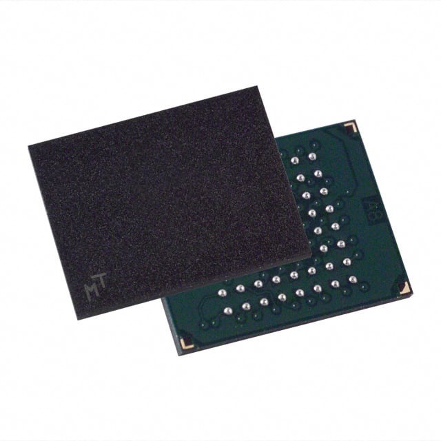
MT28F640J3BS-115 GMET
| Part Description |
IC FLASH 64MBIT PARALLEL 64FBGA |
|---|---|
| Quantity | 1,206 Available (as of June 14, 2026) |
| Product Category | Memory |
|---|---|
| Manufacturer | Micron Technology Inc. |
| Manufacturing Status | Obsolete |
| Manufacturer Standard Lead Time | Contact Us |
| Datasheet |
Specifications & Environmental
| Device Package | 64-FBGA (10x13) | Memory Format | FLASH | Technology | FLASH | ||
|---|---|---|---|---|---|---|---|
| Memory Size | 64 Mbit | Access Time | 115 ns | Grade | Industrial | ||
| Clock Frequency | N/A | Voltage | 2.7V ~ 3.6V | Memory Type | Non-Volatile | ||
| Operating Temperature | -40°C ~ 85°C (TA) | Write Cycle Time Word Page | N/A | Packaging | 64-FBGA | ||
| Mounting Method | Non-Volatile | Memory Interface | Parallel | Memory Organization | 8M x 8, 4M x 16 | ||
| Moisture Sensitivity Level | 2 (1 Year) | RoHS Compliance | ROHS3 Compliant | REACH Compliance | REACH Unaffected | ||
| Qualification | N/A | ECCN | 3A991B1A | HTS Code | 8542.32.0071 |
Overview of MT28F640J3BS-115 GMET – 64Mbit Parallel Flash, 64‑FBGA
The MT28F640J3BS-115 GMET is a 64 Mbit non-volatile FLASH memory device in a 64-ball FBGA package. It implements Micron's Q-FLASH architecture with parallel interface options and is available in x8 and x16 memory organizations.
This device targets designs that require parallel-access FLASH storage with a VCC range of 2.7 V to 3.6 V, a 115 ns read access time, and extended operating temperature from -40°C to 85°C. Key value attributes include block-level erase architecture, write-buffer programming performance, and on-device protection features.
Key Features
- Memory Core & Organization 64 Mbit FLASH available in 8M × 8 and 4M × 16 organizations with sixty-four 128 KB erase blocks (64 Mb device).
- Interface Parallel memory interface with industry-standard pinout and fully TTL-compatible inputs/outputs.
- Performance / Timing 115 ns read access time (device timing option -115) with asynchronous page mode reads and read access timings documented in the datasheet.
- Power Supply VCC, VCCQ, and VPEN operate from 2.7 V to 3.6 V for normal operation and application programming.
- Program & Erase Automatic write and erase algorithms, 5.6 μs-per-byte effective programming time using the write buffer, and 100,000 erase cycles per block.
- Protection & Security 128-bit protection register, 64-bit unique device identifier, 64-bit user-programmable OTP cells, and enhanced data protection features (e.g., VPEN = VSS options and flexible sector locking).
- Suspend / Resume Options Block erase suspend-to-read, block erase suspend-to-program, and program suspend-to-read allow interruptible operations for concurrent access scenarios.
- Package & Temperature 64-ball FBGA (10 × 13 mm ball array, 1.00 mm pitch) with operating temperature range of -40°C to +85°C (TA).
- Standards & Query Supports Common Flash Interface (CFI) and Scalable Command Set for system identification and configuration.
Typical Applications
- Embedded non-volatile storage Parallel FLASH storage for systems requiring block-erasable non-volatile memory in a compact FBGA footprint.
- Code and data storage Storage of firmware, lookup tables, or fixed data in systems that use a parallel memory interface and require extended temperature operation.
- Systems needing interruptible memory operations Designs that benefit from erase/program suspend features to allow read or program operations during long erase cycles.
Unique Advantages
- Parallel interface compatibility: Parallel access and industry-standard pinout simplify integration into existing parallel-memory designs.
- Block-level erase granularity: Sixty-four 128 KB erase blocks provide deterministic erase boundaries for partitioned storage and code/data management.
- Robust endurance: Specified for 100,000 erase cycles per block to support repeated reprogramming in field-updatable applications.
- Fast effective programming with write buffer: 5.6 μs-per-byte effective programming time using the device write buffer reduces programming time compared with byte-by-byte programming.
- On-device identification and protection: 64-bit unique ID, 64-bit OTP cells, and a 128-bit protection register enable device authentication and configurable protection schemes.
- Wide supply and temperature range: 2.7 V–3.6 V supply operation and -40°C to +85°C temperature range support a range of embedded system environments.
Why Choose IC FLASH 64MBIT PARALLEL 64FBGA?
The IC FLASH 64MBIT PARALLEL 64FBGA (MT28F640J3BS-115 GMET) provides a balanced combination of parallel-access performance, block-erase flexibility, and on-chip protection features in a compact 64-ball FBGA package. Its 115 ns read timing, write-buffer programming efficiency, and extensive suspend/resume options make it suitable for systems that require predictable non-volatile storage behavior and interruptible operations.
Backed by Micron Technology Inc.'s Q-FLASH architecture and CFI support, this device is appropriate for designers specifying a 64 Mbit parallel FLASH solution with defined endurance, unique device identification, and extended temperature operation. It delivers a verifiable, specification-driven choice for embedded designs that need parallel FLASH memory in a 64-FBGA form factor.
Request a quote or submit a request for pricing and availability to evaluate the MT28F640J3BS-115 GMET for your design needs.