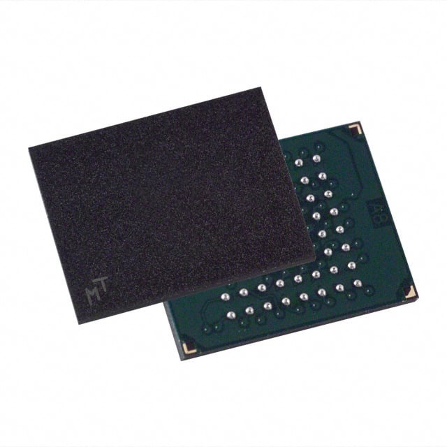
MT28F640J3BS-115 MET
| Part Description |
IC FLASH 64MBIT PARALLEL 64FBGA |
|---|---|
| Quantity | 141 Available (as of June 15, 2026) |

| Product Category | Memory |
|---|---|
| Manufacturer | Micron Technology Inc. |
| Manufacturing Status | Obsolete |
| Manufacturer Standard Lead Time | Contact Us |
| Datasheet |
Specifications & Environmental
| Device Package | 64-FBGA (10x13) | Memory Format | FLASH | Technology | FLASH | ||
|---|---|---|---|---|---|---|---|
| Memory Size | 64 Mbit | Access Time | 115 ns | Grade | Industrial | ||
| Clock Frequency | N/A | Voltage | 2.7V ~ 3.6V | Memory Type | Non-Volatile | ||
| Operating Temperature | -40°C ~ 85°C (TA) | Write Cycle Time Word Page | N/A | Packaging | 64-FBGA | ||
| Mounting Method | Non-Volatile | Memory Interface | Parallel | Memory Organization | 8M x 8, 4M x 16 | ||
| Moisture Sensitivity Level | 2 (1 Year) | RoHS Compliance | ROHS3 Compliant | REACH Compliance | REACH Unaffected | ||
| Qualification | N/A | ECCN | 3A991B1A | HTS Code | 8542.32.0071 |
Overview of MT28F640J3BS-115 MET – IC FLASH 64MBIT PARALLEL 64FBGA
The MT28F640J3BS-115 MET is a 64 Mbit non-volatile FLASH memory device with a parallel interface and a 64-ball FBGA package. It implements NOR-style Q-FLASH architecture with x8/x16 memory organization and is optimized for systems that require reliable parallel flash storage with fast read access.
Key device characteristics include a 115 ns read access time (64Mb option), 2.7 V to 3.6 V supply range, and an extended operating temperature range of -40°C to +85°C, making it suitable for designs that demand robust non-volatile code or data storage in compact BGA form factors.
Key Features
- Memory Core and Organization 64 Mbit FLASH offered in x8/x16 organization (8M × 8 or 4M × 16) with sixty-four 128 KB erase blocks for the 64Mb device.
- Performance 115 ns asynchronous page mode read access time for the 64Mb device, plus a 25 ns secondary read timing for page-mode operations.
- Power VCC, VCCQ, and VPEN operate from 2.7 V to 3.6 V, supporting typical 3.0 V system supplies and application programming within the same range.
- Package 64-ball FBGA package (10 × 13 mm) in a compact footprint for high-density board designs.
- Endurance and Data Protection Up to 100,000 erase cycles per block and enhanced data protection features including a 128-bit protection register, flexible sector locking, and sector erase/program lockout during power transitions.
- Programming and Reliability Automatic write and erase algorithms with a 5.6 µs-per-byte effective programming time using the write buffer; automatic suspend options for erase/program operations (suspend-to-read, suspend-to-program).
- Identification and Security 64-bit unique device identifier and 64-bit user-programmable OTP cells for device tracking and one-time programmable data; Common Flash Interface (CFI) and Scalable Command Set supported.
- Compatibility and Interface Industry-standard pinout with fully TTL-compatible inputs and outputs for straightforward integration into parallel-memory systems.
Typical Applications
- Firmware and code storage — Store executable code and firmware where 64 Mbit density, parallel access, and 115 ns read performance are required.
- System boot and BIOS — Use as non-volatile boot/storage memory in systems that require a compact FBGA package and industry-standard pinout.
- Embedded storage — Retain configuration, calibration, or application data in designs that need OTP capability and unique device identification.
Unique Advantages
- Direct parallel integration: Parallel interface and industry-standard pinout enable straightforward replacement or integration into existing parallel-memory designs.
- Robust erase block architecture: Sixty-four 128 KB erase blocks (for the 64Mb device) simplify block-level management and sector locking strategies.
- Enhanced data protection: Protection register, flexible sector locking, OTP cells, and an enhanced VPEN protection option reduce the risk of unintended modification.
- Fast effective programming: Write-buffer programming delivers a 5.6 µs-per-byte effective programming time for efficient in-system updates.
- Extended temperature operation: Specified for -40°C to +85°C operation to support designs requiring a wide ambient temperature range.
- High endurance: Rated for 100,000 erase cycles per block to support field updates and long-term use.
Why Choose MT28F640J3BS-115 MET?
The MT28F640J3BS-115 MET combines a parallel NOR FLASH architecture, compact 64-ball FBGA packaging, and a suite of data protection and programming features to deliver dependable non-volatile storage for systems that require 64 Mbit density and predictable read/program behavior. Its 2.7 V–3.6 V supply range, 115 ns read access (64Mb), and extended -40°C to +85°C operating range position it for designs that need stable operation across a range of conditions.
This device is suited to engineers specifying parallel flash for firmware, boot code, and embedded data storage where block-level control, device identification, and programming performance are important design considerations. Built-in protection mechanisms and automatic programming/erase algorithms support maintainability and reliability over the product life cycle.
Request a quote or submit an inquiry to discuss availability, pricing, and delivery for the MT28F640J3BS-115 MET.