MT28F640J3RG-115 ET TR
| Part Description |
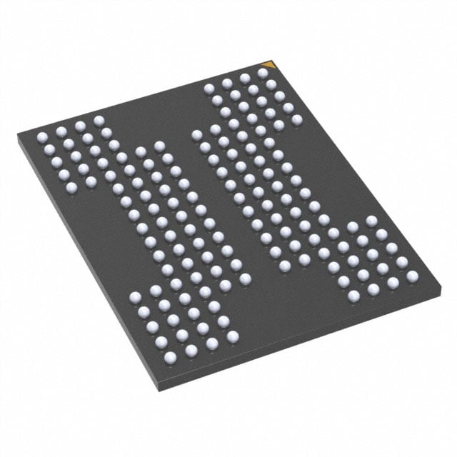
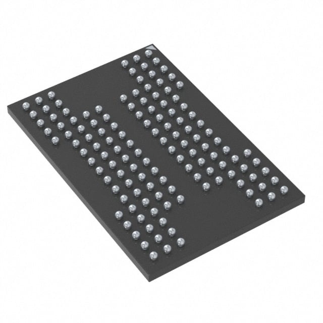
IC FLASH 64MBIT PARALLEL 56TSOP |
|---|---|
| Quantity | 678 Available (as of June 9, 2026) |

| Product Category | Memory |
|---|---|
| Manufacturer | Micron Technology Inc. |
| Manufacturing Status | Obsolete |
| Manufacturer Standard Lead Time | Contact Us |
| Datasheet |
Specifications & Environmental
| Device Package | 56-TSOP | Memory Format | FLASH | Technology | FLASH | ||
|---|---|---|---|---|---|---|---|
| Memory Size | 64 Mbit | Access Time | 115 ns | Grade | Industrial | ||
| Clock Frequency | N/A | Voltage | 2.7V ~ 3.6V | Memory Type | Non-Volatile | ||
| Operating Temperature | -40°C ~ 85°C (TA) | Write Cycle Time Word Page | N/A | Packaging | 56-TFSOP (0.724", 18.40mm Width) | ||
| Mounting Method | Non-Volatile | Memory Interface | Parallel | Memory Organization | 8M x 8, 4M x 16 | ||
| Moisture Sensitivity Level | 3 (168 Hours) | RoHS Compliance | RoHS non-compliant | REACH Compliance | REACH Unaffected | ||
| Qualification | N/A | ECCN | 3A991B1A | HTS Code | 8542.32.0071 |
Overview of MT28F640J3RG-115 ET TR – IC FLASH 64MBIT PARALLEL 56TSOP
The MT28F640J3RG-115 ET TR is a 64 Mbit non-volatile Flash memory device in a 56-pin TSOP Type I package. It implements a parallel memory interface with x8/x16 organization and supports industry-standard command sets and query structures.
Designed for systems requiring parallel Flash storage, the device offers 115 ns read access, 2.7 V to 3.6 V operation, and extended temperature operation from -40°C to +85°C, delivering a combination of predictable timing, data protection features, and block-level erase/program control.
Key Features
- Memory Capacity & Organization — 64 Mbit total capacity provided as 8M × 8 or 4M × 16 configurations, with sixty-four 128 KB erase blocks for block-level management.
- Performance — 115 ns asynchronous read access time for the 64 Mbit device; supports asynchronous page mode reads for system efficiency.
- Voltage & Programming — Operates from 2.7 V to 3.6 V for both VCC and application programming; includes an automatic write and erase algorithm and write-buffer programming (effective programming time specified at 5.6 μs per byte using the write buffer).
- Interface & Compatibility — Parallel memory interface with industry-standard pinout and fully TTL-compatible inputs and outputs; supports Common Flash Interface (CFI) and a Scalable Command Set for system integration and identification.
- Data Protection & Security — Enhanced data protection features including VPEN = VSS option, flexible sector locking, a 128-bit protection register, a 64-bit unique device identifier, and 64-bit user-programmable OTP cells.
- Reliability & Endurance — Endurance characterized with 100,000 erase cycles per block and automatic suspend options (Block Erase Suspend-to-Read, Block Erase Suspend-to-Program, Program Suspend-to-Read) to support interruptible operations.
- Package & Temperature — Supplied in a 56-pin TSOP (56-TFSOP / 56-TSOP) with 0.724" (18.40 mm) width; rated for extended ambient operation from -40°C to +85°C (ET option).
Typical Applications
- Embedded firmware storage — Non-volatile code and configuration storage for systems that require a parallel Flash interface and block-level erase/program control.
- Boot and system code — Storage of bootloaders and system firmware where defined read access time (115 ns) and CFI-compatible identification are required.
- Field upgradeable devices — Devices that use sector locking, OTP cells, and suspend-to-read/program features to manage in-field programming and updates.
Unique Advantages
- CFI and standard command support: Enables straightforward device identification and integration using the Common Flash Interface and a scalable command set.
- Flexible memory organization: x8/x16 options and 128 KB erase blocks allow designers to match data-width and block-size requirements to application needs.
- Robust data protection: Built-in protection register, unique device ID, OTP cells, and sector locking provide multiple layers of data integrity and security control.
- Interruptible operations: Block erase and program suspend options permit read operations during long erase/program cycles, improving system responsiveness.
- Qualified endurance: Up to 100,000 erase cycles per block supports long-term program/erase lifecycles for persistent storage.
Why Choose MT28F640J3RG-115 ET TR?
The MT28F640J3RG-115 ET TR combines a 64 Mbit parallel Flash architecture with comprehensive data-protection features, predictable 115 ns read timing, and extended temperature operation, making it suitable for designs that require reliable non-volatile storage with block-level control. Industry-standard pinout and CFI support simplify system integration and device identification.
This device is appropriate for engineers specifying parallel Flash for firmware, boot code, and field-upgradeable storage where endurance, suspend capabilities, and secure programming options are important. Its package and voltage range provide options for a range of board-level implementations while retaining the block-management and protection features documented in the datasheet.
Request a quote or contact sales to discuss part availability, pricing, and lead times for the MT28F640J3RG-115 ET TR.