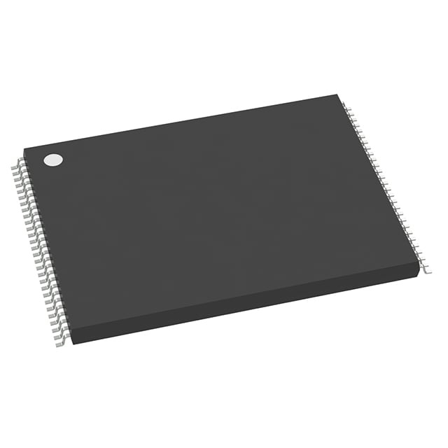
MT28F128J3RP-12 ET TR
| Part Description |
IC FLASH 128MBIT PARALLEL 56TSOP |
|---|---|
| Quantity | 83 Available (as of June 15, 2026) |

| Product Category | Flash Memory |
|---|---|
| Manufacturer | Micron Technology Inc. |
| Manufacturing Status | Obsolete |
| Manufacturer Standard Lead Time | Contact Us |
| Datasheet |
Specifications & Environmental
| Device Package | 56-TSOP | Memory Format | FLASH | Technology | FLASH | ||
|---|---|---|---|---|---|---|---|
| Memory Size | 128 Mbit | Access Time | 120 ns | Grade | Industrial | ||
| Clock Frequency | N/A | Voltage | 2.7V ~ 3.6V | Memory Type | Non-Volatile | ||
| Operating Temperature | -40°C ~ 85°C (TA) | Write Cycle Time Word Page | N/A | Packaging | 56-TFSOP (0.724", 18.40mm Width) | ||
| Mounting Method | Non-Volatile | Memory Interface | Parallel | Memory Organization | 16M x 8, 8M x 16 | ||
| Moisture Sensitivity Level | 4 (72 Hours) | RoHS Compliance | ROHS3 Compliant | REACH Compliance | REACH Unaffected | ||
| Qualification | N/A | ECCN | 3A991B1A | HTS Code | 8542.32.0071 |
Overview of MT28F128J3RP-12 ET TR – IC FLASH 128Mbit Parallel 56-TSOP
The MT28F128J3RP-12 ET TR is a 128 Mbit Q‑FLASH® non-volatile FLASH memory device in a 56‑pin TSOP Type I package. It provides parallel read/write access with x8/x16 memory organization and industry-standard pinout.
Designed for system code and data storage, the device delivers deterministic read access (120 ns), wide supply range (2.7 V to 3.6 V), extended operating temperature (‑40 °C to +85 °C), and on-chip protection and management features for reliable field operation.
Key Features
- Memory Core 128 Mbit FLASH organized as 16M × 8 or 8M × 16 with one hundred twenty 128 KB erase blocks.
- Performance Asynchronous page-mode reads with 120 ns primary read access time (128 Mb device) and 25 ns page-mode timing.
- Supply and Programming Operates and programs from 2.7 V to 3.6 V; supports application programming at the same voltage range.
- Endurance and Reliability Rated for 100,000 erase cycles per block with automatic write and erase algorithms and automatic suspend options for erase/program operations.
- Protection and Security 128‑bit protection register, 64‑bit unique device identifier, 64‑bit user-programmable OTP cells, and enhanced data protection when VPEN = VSS.
- Programming Efficiency Write buffer supports effective programming throughput (5.6 μs per byte effective programming time using the write buffer).
- Interface and Compatibility Parallel memory interface with fully TTL‑compatible inputs/outputs, Common Flash Interface (CFI), and Scalable Command Set for system integration.
- Package and Temperature 56‑pin TSOP Type I (56‑TFSOP, 18.40 mm width) in extended temperature option (‑40 °C to +85 °C ET).
Typical Applications
- Embedded system code storage Non‑volatile storage of firmware and boot code in systems requiring parallel flash memory.
- Industrial equipment Extended temperature range and robust erase/program endurance suit industrial controllers and instrumentation.
- Field upgradeable products CFI and Scalable Command Set support in‑system firmware updates and device identification for upgrade workflows.
Unique Advantages
- Extended temperature support: Operation from ‑40 °C to +85 °C enables deployment in temperature-challenging environments.
- Flexible data organization: x8 and x16 memory organization options simplify bus integration across different system designs.
- Fast, deterministic reads: 120 ns read access time provides predictable performance for code execution and data fetch.
- Robust data protection: On-chip protection register, unique ID, and OTP cells allow device-level security and identification features.
- High endurance: 100,000 erase cycles per block and automatic suspend options improve reliability for frequent update scenarios.
Why Choose MT28F128J3RP-12 ET TR?
The MT28F128J3RP-12 ET TR combines a 128 Mbit Q‑FLASH architecture with parallel interface flexibility, extended temperature range, and proven protection features to address embedded storage needs where reliability and deterministic access matter. Its voltage range (2.7 V–3.6 V), program/erase robustness, and programming efficiency via a write buffer make it suitable for designs that require stable, field‑maintainable non‑volatile memory.
This device is well suited to engineers and procurement teams specifying parallel FLASH for firmware storage, in‑field upgrade support, and industrial applications where temperature and endurance requirements are explicit. The included CFI and Scalable Command Set support system integration and device identification in complex designs.
Request a quote or submit a pricing and lead-time inquiry using the MT28F128J3RP-12 ET TR part number to get detailed availability and ordering information.