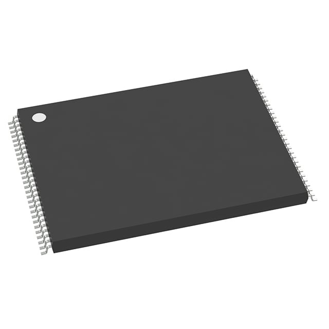
MT28F128J3RP-12 ET
| Part Description |
IC FLASH 128MBIT PARALLEL 56TSOP |
|---|---|
| Quantity | 107 Available (as of June 15, 2026) |

| Product Category | Memory |
|---|---|
| Manufacturer | Micron Technology Inc. |
| Manufacturing Status | Obsolete |
| Manufacturer Standard Lead Time | Contact Us |
| Datasheet |
Specifications & Environmental
| Device Package | 56-TSOP | Memory Format | FLASH | Technology | FLASH | ||
|---|---|---|---|---|---|---|---|
| Memory Size | 128 Mbit | Access Time | 120 ns | Grade | Industrial | ||
| Clock Frequency | N/A | Voltage | 2.7V ~ 3.6V | Memory Type | Non-Volatile | ||
| Operating Temperature | -40°C ~ 85°C (TA) | Write Cycle Time Word Page | N/A | Packaging | 56-TFSOP (0.724", 18.40mm Width) | ||
| Mounting Method | Non-Volatile | Memory Interface | Parallel | Memory Organization | 16M x 8, 8M x 16 | ||
| Moisture Sensitivity Level | 4 (72 Hours) | RoHS Compliance | ROHS3 Compliant | REACH Compliance | REACH Unaffected | ||
| Qualification | N/A | ECCN | 3A991B1A | HTS Code | 8542.32.0071 |
Overview of MT28F128J3RP-12 ET – IC FLASH 128MBIT PARALLEL 56TSOP
The MT28F128J3RP-12 ET is a 128 Mbit non-volatile FLASH memory device manufactured by Micron Technology, Inc., delivered in a 56-pin TSOP Type I package. It provides parallel memory access with x8/x16 organization and is designed for systems requiring parallel FLASH storage with defined block geometry and command support.
Key characteristics include a 16M × 8 or 8M × 16 memory organization, asynchronous page-mode read support, a 2.7 V to 3.6 V supply range for operation and programming, and an extended operating temperature range of −40°C to +85°C.
Key Features
- Memory Capacity & Organization 128 Mbit total capacity with memory organization options of 16M × 8 or 8M × 16 and one hundred twenty-eight 128 KB erase blocks for structured block management.
- Non-Volatile FLASH Technology Standard FLASH memory technology providing persistent storage without battery backup.
- Performance & Read Timing Asynchronous page-mode read support with 120 ns / 25 ns read access time specified for the 128 Mb device.
- Voltage & Programming Operates and programs at VCC = 2.7 V to 3.6 V; effective programming using the write buffer yields approximately 5.6 μs-per-byte programming performance.
- Interface & Compatibility Parallel memory interface with an industry-standard pinout and fully TTL-compatible inputs and outputs; supports Common Flash Interface (CFI) and the Scalable Command Set.
- Protection & Security 128-bit protection register, 64-bit unique device identifier, and 64-bit user-programmable OTP cells; enhanced data protection when VPEN = VSS, plus flexible sector locking and lockout during power transitions.
- Reliability & Endurance Rated for 100,000 erase cycles per block and includes automatic write and erase algorithms and suspend/resume options (erase/program suspend-to-read and program suspend-to-read).
- Package & Temperature 56-TFSOP (56-TSOP Type I) package (0.724", 18.40 mm width) and extended ambient operating temperature range of −40°C to +85°C.
Unique Advantages
- Predictable block layout: One hundred twenty-eight 128 KB erase blocks simplify memory partitioning and firmware layout for block-based storage management.
- Wide supply range: 2.7 V to 3.6 V operation accommodates common 3 V system rails for both operation and programming.
- Improved programming throughput: Write-buffer-assisted programming achieves an effective 5.6 μs per byte, reducing programming time compared with byte-by-byte programming.
- Built-in data protection: 128-bit protection register plus sector locking and power-transition lockout help safeguard stored data and region-level access.
- High endurance: 100,000 erase cycles per block provides a reliable endurance specification for repetitive program/erase use cases.
- Standard parallel interface: Industry-standard pinout and TTL-compatible I/Os enable straightforward integration into parallel-memory system designs.
Why Choose IC FLASH 128MBIT PARALLEL 56TSOP?
The MT28F128J3RP-12 ET offers a combination of defined block geometry, parallel-interface performance, and robust protection features suitable for designs that require structured non-volatile storage with extended temperature operation. Its voltage flexibility, write-buffer programming efficiency, and endurance characteristics make it appropriate for systems that need repeatable block erase/program cycles and secure region management.
This device is suited to engineers and procurement teams specifying a 128 Mbit parallel FLASH in a 56-pin TSOP footprint who require explicit endurance, timing, and protection details for system-level memory planning and integration.
Request a quote or submit a product inquiry for the MT28F128J3RP-12 ET to receive pricing, lead-time, and availability information.