MT48LC128M4A2TG-75:C TR
| Part Description |
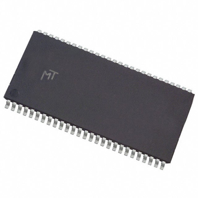
IC DRAM 512MBIT PAR 54TSOP II |
|---|---|
| Quantity | 777 Available (as of June 15, 2026) |
| Product Category | DRAM Memory |
|---|---|
| Manufacturer | Micron Technology Inc. |
| Manufacturing Status | Obsolete |
| Manufacturer Standard Lead Time | Contact Us |
| Datasheet |
Specifications & Environmental
| Device Package | 54-TSOP II | Memory Format | DRAM | Technology | SDRAM | ||
|---|---|---|---|---|---|---|---|
| Memory Size | 512 Mbit | Access Time | 5.4 ns | Grade | Commercial | ||
| Clock Frequency | 133 MHz | Voltage | 3V ~ 3.6V | Memory Type | Volatile | ||
| Operating Temperature | 0°C ~ 70°C (TA) | Write Cycle Time Word Page | 15 ns | Packaging | 54-TSOP (0.400", 10.16mm Width) | ||
| Mounting Method | Volatile | Memory Interface | Parallel | Memory Organization | 128M x 4 | ||
| Moisture Sensitivity Level | 4 (72 Hours) | RoHS Compliance | RoHS non-compliant | REACH Compliance | REACH Unaffected | ||
| Qualification | N/A | ECCN | EAR99 | HTS Code | 8542.32.0024 |
Overview of MT48LC128M4A2TG-75:C TR – IC DRAM 512MBIT PAR 54TSOP II
The MT48LC128M4A2TG-75:C TR is a 512 Mbit synchronous DRAM (SDRAM) organized as 128M × 4 with a parallel memory interface in a 54‑pin TSOP II package. It implements fully synchronous, pipelined operation with internal banks and programmable burst lengths for deterministic, clock‑aligned memory transfers.
Targeted for designs requiring a 3.3 V single‑supply SDRAM solution, this -75 speed grade supports up to 133 MHz clocking with a 5.4 ns access time at CL = 3 and operates over a commercial temperature range of 0 °C to 70 °C.
Key Features
- Memory Core 512 Mbit SDRAM organized as 128M × 4 with internal, multi‑bank architecture (4 banks) to hide row access/precharge and support concurrent operations.
- Synchronous, Pipelined Operation Fully synchronous device with all signals registered on the positive edge of the system clock and internal pipelining that allows column addresses to change every clock cycle.
- Performance and Timing PC100 and PC133 compliant; -75 speed grade supports 133 MHz clock frequency and 5.4 ns access time at CAS latency (CL) = 3. Write cycle time (word/page) is 15 ns.
- Programmable Burst and Refresh Programmable burst lengths of 1, 2, 4, 8, or full page; supports auto precharge, auto refresh and self refresh with a 64 ms / 8192‑cycle refresh interval.
- Electrical Single 3.3 V supply (3.0–3.6 V) with LVTTL‑compatible inputs and outputs for standard 3.3 V system integration.
- Package and Temperature 54‑pin TSOP II (400 mil, 10.16 mm width) plastic package; commercial operating temperature 0 °C to +70 °C.
Typical Applications
- PC100 / PC133 system memory Use in systems requiring PC100 or PC133 compliant synchronous DRAM with standard 3.3 V signaling.
- Compact, high‑density memory subsystems 512 Mbit density in a 54‑pin TSOP II package for space‑constrained board designs.
- Synchronous buffered memory for embedded systems Pipelined reads/writes and programmable burst lengths support predictable data flow in clocked embedded memory subsystems.
Unique Advantages
- High‑density SDRAM in a compact package: 512 Mbit capacity in a 54‑pin TSOP II (10.16 mm) simplifies layout for space‑limited designs.
- Clock‑aligned, pipelined operation: Fully synchronous design with registered inputs/outputs enables deterministic timing and supports burst‑mode transfers.
- PC100/PC133 compatibility: Speed grade and timing options align with PC100/PC133 system requirements for straightforward integration.
- Flexible refresh and power modes: Auto refresh and self refresh modes with standard 8K refresh cycles reduce external refresh management.
- Standard 3.3 V signaling: Single 3.0–3.6 V supply and LVTTL‑compatible I/O simplify power sequencing and interfacing with common logic families.
Why Choose IC DRAM 512MBIT PAR 54TSOP II?
The MT48LC128M4A2TG-75:C TR delivers a verified 512 Mbit SDRAM solution with PC100/PC133 timing, pipelined synchronous operation, and programmable burst capabilities suited to designs that need predictable, clocked memory performance in a compact TSOP II package. Its commercial temperature rating and standard 3.3 V supply make it appropriate for a broad range of board‑level memory subsystems.
This part is appropriate for engineers specifying a parallel SDRAM device where density, burst‑transfer performance, and a 54‑pin TSOP II footprint are required. The device’s refresh, power and timing options provide design flexibility while using a widely supported SDRAM architecture.
If you would like pricing, availability, or to request a quote for MT48LC128M4A2TG-75:C TR, please request a quote or contact sales to discuss requirements and lead times.