MT48LC16M16A2FG-7E:D TR
| Part Description |
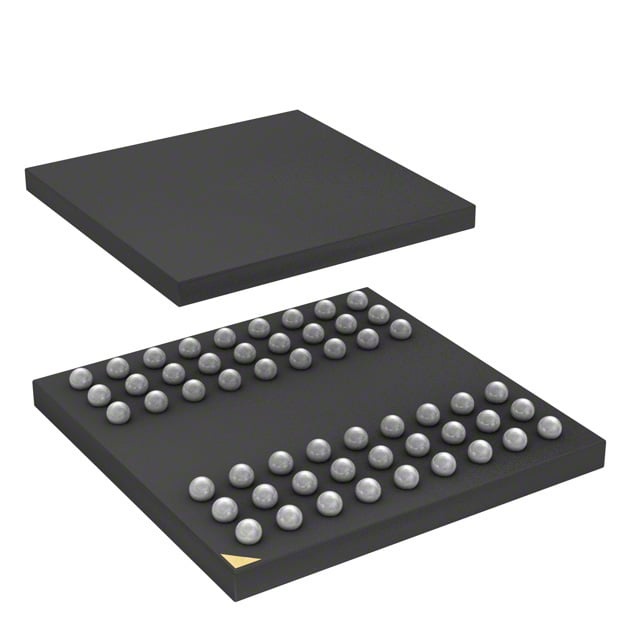
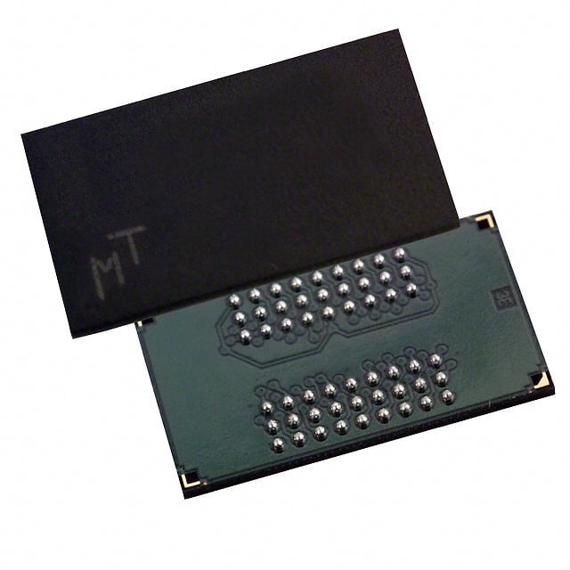
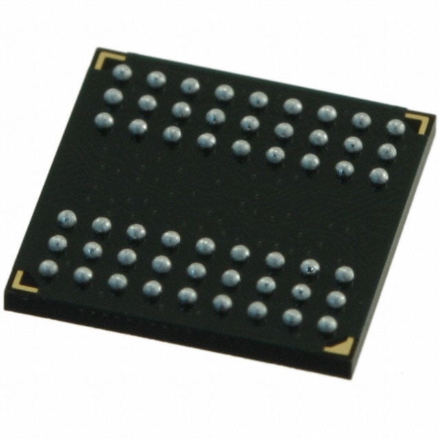
IC DRAM 256MBIT PAR 54VFBGA |
|---|---|
| Quantity | 1,010 Available (as of June 15, 2026) |
| Product Category | Memory |
|---|---|
| Manufacturer | Micron Technology Inc. |
| Manufacturing Status | Obsolete |
| Manufacturer Standard Lead Time | Contact Us |
| Datasheet |
Specifications & Environmental
| Device Package | 54-VFBGA (8x14) | Memory Format | DRAM | Technology | SDRAM | ||
|---|---|---|---|---|---|---|---|
| Memory Size | 256 Mbit | Access Time | 5.4 ns | Grade | Commercial | ||
| Clock Frequency | 133 MHz | Voltage | 3V ~ 3.6V | Memory Type | Volatile | ||
| Operating Temperature | 0°C ~ 70°C (TA) | Write Cycle Time Word Page | 14 ns | Packaging | 54-VFBGA | ||
| Mounting Method | Volatile | Memory Interface | Parallel | Memory Organization | 16M x 16 | ||
| Moisture Sensitivity Level | 3 (168 Hours) | RoHS Compliance | ROHS3 Compliant | REACH Compliance | REACH Unaffected | ||
| Qualification | N/A | ECCN | EAR99 | HTS Code | 8542.32.0024 |
Overview of MT48LC16M16A2FG-7E:D TR – IC DRAM 256Mbit Parallel 54-VFBGA
The MT48LC16M16A2FG-7E:D TR is a 256 Mbit SDRAM device organized as 16M × 16 with internal bank architecture and a parallel memory interface. It implements fully synchronous, pipelined SDRAM architecture and is offered in a 54-ball VFBGA package.
Designed for systems requiring PC100/PC133-compliant SDRAM timing, this device emphasizes synchronous, pipelined operation, programmable burst lengths and standard refresh modes to support memory subsystems in compact board-level applications operating within a commercial temperature range.
Key Features
- Memory Core & Organization 256 Mbit SDRAM organized as 16M × 16, internally arranged as 4M × 16 × 4 banks to support multi-bank operation and hidden row access/precharge.
- Interface & Timing Parallel SDRAM interface with a 133 MHz clock frequency (–7E speed grade). Timing examples for the –7E grade include 2-2-2 RCD-RP-CL and CAS latency characteristics specified in the datasheet.
- Performance & Operation Fully synchronous, internal pipelined operation that allows column address changes every clock cycle, programmable burst lengths (1, 2, 4, 8, or full page), auto precharge and auto refresh.
- Power Single power supply operation at 3.3 V ±0.3 V (specified voltage range 3.0 V to 3.6 V).
- I/O LVTTL-compatible inputs and outputs for standard logic-level interfacing.
- Timing Metrics Access time listed at 5.4 ns and write cycle time (word page) of 14 ns for the specified device.
- Refresh Supports standard auto refresh and self-refresh modes with 8192-cycle refresh; commercial refresh interval specified as 64 ms for 8K cycles.
- Package & Temperature 54-ball VFBGA package (8 × 14 mm footprint) with an operating temperature range of 0°C to 70°C (TA), suitable for commercial-temperature applications.
Typical Applications
- PC100/PC133 memory subsystems — Use where PC100- and PC133-compliant SDRAM timing is required for legacy or compatible systems.
- Board-level parallel memory — Compact 54-ball VFBGA package enables integration of 256 Mbit parallel SDRAM on space-constrained PCBs.
- Commercial electronic equipment — Memory for systems operating within the 0°C to 70°C commercial temperature range that require standard SDRAM refresh and burst capabilities.
- Module and add-on designs — Suitable for memory expansion or substitute devices in modules that specify 16M × 16 organization and a 3.3 V supply.
Unique Advantages
- PC100/PC133 compliance: Provides timing compatibility with PC100 and PC133 system requirements as documented for the 256Mb product family.
- Synchronous, pipelined architecture: Fully synchronous operation with internal pipelining and multi-bank organization helps maintain steady throughput by allowing column address changes every clock cycle.
- Flexible burst control: Programmable burst lengths (1, 2, 4, 8, full page) let designers tailor transfers for sequential or random-access patterns.
- Compact VFBGA package: 54-ball VFBGA (8 × 14 mm) reduces PCB footprint for board-level memory integration.
- Standard 3.3 V supply: Operates from a single 3.0 V–3.6 V supply (3.3 V ±0.3 V), simplifying power rail requirements.
- Commercial temperature support: Rated for 0°C to 70°C operation and standard 64 ms/8192-cycle refresh for commercial applications.
Why Choose MT48LC16M16A2FG-7E:D TR?
The MT48LC16M16A2FG-7E:D TR is positioned for designs that need a compact, PC100/PC133-compatible 256 Mbit SDRAM with synchronous, pipelined operation and flexible burst and refresh features. Its 16M × 16 organization, multi-bank architecture and LVTTL I/O make it suitable for board-level memory implementations where standardized timing and a 3.3 V supply are required.
This device is a practical choice for commercial-temperature memory subsystems that require predictable SDRAM behavior—programmable burst lengths, auto-refresh/self-refresh support and an industry-standard VFBGA footprint help integrate 256 Mbit of parallel SDRAM into space-constrained designs while meeting common system timing expectations.
Request a quote or submit a pricing inquiry to begin sourcing MT48LC16M16A2FG-7E:D TR for your next design.