MT48LC16M16A2FG-75:D TR
| Part Description |
IC DRAM 256MBIT PAR 54VFBGA |
|---|---|
| Quantity | 819 Available (as of June 15, 2026) |

| Product Category | Memory |
|---|---|
| Manufacturer | Micron Technology Inc. |
| Manufacturing Status | Obsolete |
| Manufacturer Standard Lead Time | Contact Us |
| Datasheet |
Specifications & Environmental
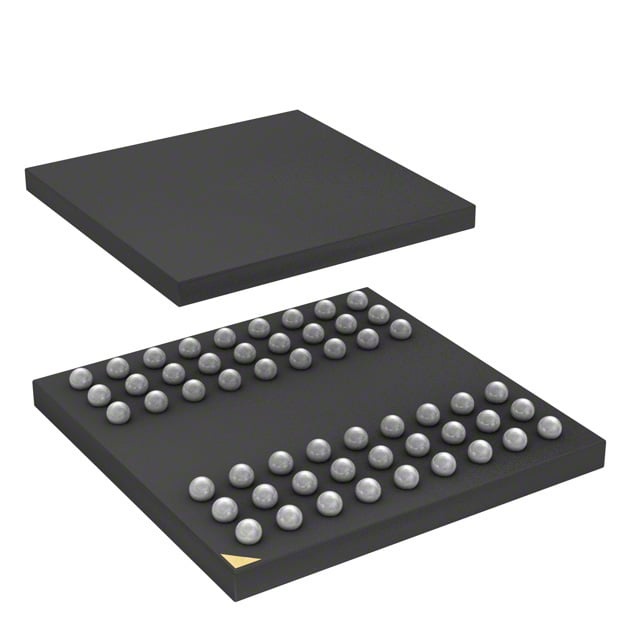
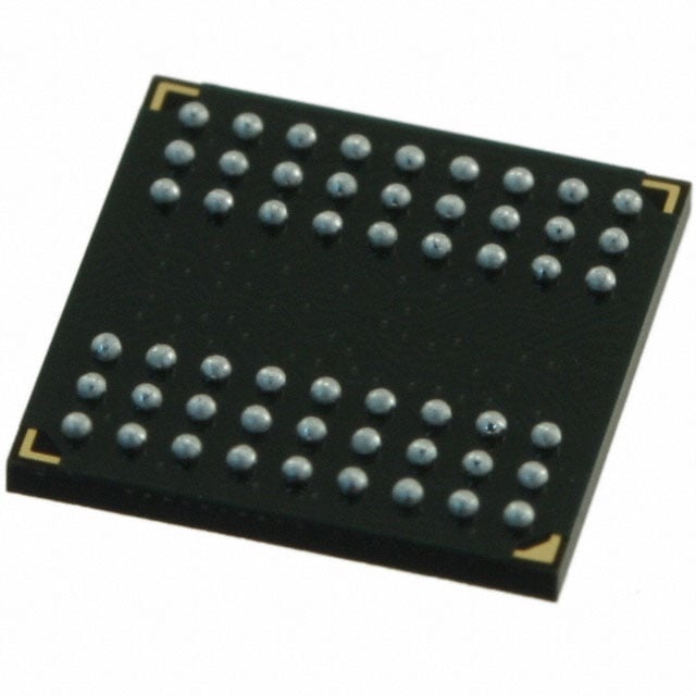
| Device Package | 54-VFBGA (8x14) | Memory Format | DRAM | Technology | SDRAM | ||
|---|---|---|---|---|---|---|---|
| Memory Size | 256 Mbit | Access Time | 5.4 ns | Grade | Commercial | ||
| Clock Frequency | 133 MHz | Voltage | 3V ~ 3.6V | Memory Type | Volatile | ||
| Operating Temperature | 0°C ~ 70°C (TA) | Write Cycle Time Word Page | 15 ns | Packaging | 54-VFBGA | ||
| Mounting Method | Volatile | Memory Interface | Parallel | Memory Organization | 16M x 16 | ||
| Moisture Sensitivity Level | 3 (168 Hours) | RoHS Compliance | RoHS non-compliant | REACH Compliance | REACH Unaffected | ||
| Qualification | N/A | ECCN | EAR99 | HTS Code | 8542.32.0024 |
Overview of MT48LC16M16A2FG-75:D TR – IC DRAM 256MBIT PAR 54VFBGA
The MT48LC16M16A2FG-75:D TR is a 256 Mbit synchronous DRAM device organized as 16M × 16 with four internal banks. It implements a fully synchronous parallel SDRAM architecture suitable for systems requiring PC100/PC133-class parallel memory.
With a 133 MHz clock frequency, 3.0–3.6 V supply range, and a 54-ball VFBGA (8×14) package, this device addresses commercial embedded and legacy memory subsystems that need predictable synchronous performance and compact board-level integration.
Key Features
- Memory Architecture 256 Mbit DRAM organized as 16M × 16 with four internal banks for concurrent row access/precharge and pipelined operation.
- Synchronous SDRAM and Compliance Fully synchronous SDRAM that is PC100- and PC133-compliant, with all signals registered on the positive edge of the system clock.
- Performance 133 MHz clock frequency (speed grade -75) with an access time of 5.4 ns and documented CAS/RAS timing targets (3-3-3 at -75 speed grade).
- Burst and Refresh Options Programmable burst lengths (1, 2, 4, 8, or full page), auto precharge, auto refresh and self-refresh modes (self-refresh not available on AT devices, per datasheet).
- Interface and I/O Parallel memory interface with LVTTL-compatible inputs and outputs for standard synchronous control signaling.
- Timing and Write Cycle Write cycle time (word/page) listed at 15 ns; timing parameters and CAS latency options supported per datasheet tables.
- Power and Operating Range Single 3.0 V to 3.6 V supply (standard 3.3 V ±0.3 V operation) and commercial operating temperature range of 0°C to +70°C (TA).
- Package 54-ball VFBGA package (8 mm × 14 mm) for high-density board mounting and compact footprint.
Typical Applications
- Embedded system memory Use as synchronous parallel DRAM for commercial embedded platforms that require PC100/PC133-class memory interfaces.
- Legacy PC/board-level subsystems Suitable for designs that implement parallel SDRAM memory subsystems compliant with PC100/PC133 timing.
- Graphics and frame buffering Works as a compact frame buffer or temporary storage in systems needing pipelined, burst-capable DRAM access.
- Networking and buffering Appropriate for packet buffering or temporary data storage in commercial networking equipment operating within the specified voltage and temperature ranges.
Unique Advantages
- PC100/PC133 compatibility: Documented compliance with PC100 and PC133 timing targets enables straightforward integration into matched system memory buses.
- Synchronous, pipelined operation: Fully synchronous design with internal pipelining and multiple banks supports continuous column-address changes every clock cycle for consistent throughput.
- Flexible burst modes: Programmable burst lengths (1, 2, 4, 8, full page) allow designers to optimize transfers for latency or throughput as required by the application.
- Compact VFBGA package: 54-ball VFBGA (8×14 mm) provides a dense, board-space-efficient footprint for applications with constrained PCB area.
- Standard 3.3 V supply and commercial temp range: Single-supply 3.0–3.6 V operation and 0°C to +70°C rating match many commercial embedded environments and power rails.
Why Choose MT48LC16M16A2FG-75:D TR?
The MT48LC16M16A2FG-75:D TR delivers a compact, synchronous 256 Mbit DRAM solution with PC100/PC133-class timing, programmable burst modes, and a 54-ball VFBGA package for high-density designs. Its documented timing parameters, pipelined internal bank architecture, and standard 3.3 V supply make it a practical choice for commercial embedded systems and legacy parallel-memory subsystems that require predictable SDRAM behavior.
This device is well suited to engineers and procurement teams building compact boards that need a commercially rated, parallel SDRAM device with established timing tables and refresh/burst options detailed in the product documentation.
Request a quote or submit a pricing inquiry to obtain availability, lead-time, and volume pricing information for the MT48LC16M16A2FG-75:D TR.