MT48LC16M16A2P-75:D
| Part Description |
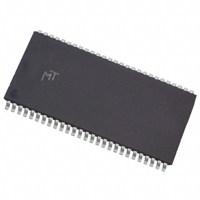
IC DRAM 256MBIT PAR 54TSOP II |
|---|---|
| Quantity | 1,953 Available (as of June 10, 2026) |

| Product Category | Memory |
|---|---|
| Manufacturer | Micron Technology Inc. |
| Manufacturing Status | Obsolete |
| Manufacturer Standard Lead Time | Contact Us |
| Datasheet |
Specifications & Environmental
| Device Package | 54-TSOP II | Memory Format | DRAM | Technology | SDRAM | ||
|---|---|---|---|---|---|---|---|
| Memory Size | 256 Mbit | Access Time | 5.4 ns | Grade | Commercial | ||
| Clock Frequency | 133 MHz | Voltage | 3V ~ 3.6V | Memory Type | Volatile | ||
| Operating Temperature | 0°C ~ 70°C (TA) | Write Cycle Time Word Page | 15 ns | Packaging | 54-TSOP (0.400", 10.16mm Width) | ||
| Mounting Method | Volatile | Memory Interface | Parallel | Memory Organization | 16M x 16 | ||
| Moisture Sensitivity Level | 3 (168 Hours) | RoHS Compliance | ROHS3 Compliant | REACH Compliance | REACH Unaffected | ||
| Qualification | N/A | ECCN | EAR99 | HTS Code | 8542.32.0024 |
Overview of MT48LC16M16A2P-75:D – IC DRAM 256MBIT PAR 54TSOP II
Micron Technology Inc. MT48LC16M16A2P-75:D is a 256 Mbit SDRAM device organized as 16M × 16 with four internal banks and a parallel memory interface. It implements synchronous DRAM architecture with pipelined operation and is offered in a 54-pin TSOP II (0.400", 10.16 mm width) package.
The device targets systems using PC100/PC133-class synchronous DRAM and provides timing and refresh features for steady, clocked memory operation at a 133 MHz speed grade.
Key Features
- Core / Architecture SDR SDRAM architecture with fully synchronous operation; all signals registered on the positive edge of the system clock and internal pipelined operation.
- Memory Organization 256 Mbit capacity organized as 16M × 16 with four internal banks, providing standard DRAM array structure for parallel access.
- Performance / Timing Speed grade -75 targets 133 MHz operation with 3-3-3 RCD-RP-CL timing (CL = 3, 20 ns). Product specification lists an access time of 5.4 ns and a write cycle time (word/page) of 15 ns.
- Interface Parallel SDRAM interface with LVTTL-compatible inputs and outputs for synchronous system integration.
- Memory Modes & Refresh Programmable burst lengths (1, 2, 4, 8, or full page), internal banks to hide row access/precharge, auto precharge, auto refresh, and self-refresh mode (self-refresh noted in family documentation; availability depends on device option).
- Power Single-supply operation at 3.0 V to 3.6 V (documented as 3.3 V ±0.3 V in family datasheet).
- Package & Temperature 54-pin TSOP II (0.400", 10.16 mm width) plastic package; commercial operating temperature range 0°C to +70°C (TA).
Typical Applications
- PC100/PC133 memory subsystems Use as synchronous DRAM on systems and modules targeting PC100/PC133-class timings and clocking.
- Embedded systems requiring parallel SDRAM Provides 256 Mbit of synchronous parallel DRAM storage for embedded designs that use a 3.3 V supply domain.
- High-density board-level memory Compact 54-pin TSOP II packaging supports dense PCB layouts where a parallel SDRAM interface is required.
Unique Advantages
- PC100/PC133 compatibility: Documented compliance with PC100 and PC133 timing classes (family datasheet), enabling integration into matching system timing environments.
- Flexible burst and banking: Programmable burst lengths and four internal banks allow continuous column access and improved throughput under synchronous operation.
- Deterministic timing at 133 MHz: Speed grade -75 provides defined RCD-RP-CL targets (3-3-3) for predictable memory timing behavior.
- Single 3.3 V supply: Operates from 3.0 V to 3.6 V, matching common system voltage rails for straightforward power integration.
- Compact TSOP II package: 54-pin TSOP II (0.400") package supports compact board area and standard surface-mount assembly.
- Manufacturer backing: Produced by Micron Technology Inc., with family-level documentation that specifies features such as auto refresh, self-refresh options, and timing parameters.
Why Choose IC DRAM 256MBIT PAR 54TSOP II?
The MT48LC16M16A2P-75:D delivers a 256 Mbit synchronous DRAM solution in a compact 54-pin TSOP II package, with PC133-class timing and internal features (burst control, internal banks, auto-refresh) suited to synchronous parallel memory designs. Its documented speed grade and timing parameters make it appropriate for systems requiring defined, clocked DRAM operation at 133 MHz.
This device is aimed at engineers specifying board-level SDRAM on a 3.3 V supply who need a parallel-interface memory with family-level features and manufacturer documentation from Micron Technology Inc.
Request a quote or contact sales to obtain pricing, availability, and lead-time information for MT48LC16M16A2P-75:D.