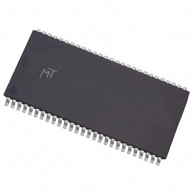
MT48LC16M8A2P-6A IT:L TR
| Part Description |
IC DRAM 128MBIT PAR 54TSOP II |
|---|---|
| Quantity | 49 Available (as of June 8, 2026) |

| Product Category | Memory |
|---|---|
| Manufacturer | Micron Technology Inc. |
| Manufacturing Status | Obsolete |
| Manufacturer Standard Lead Time | Contact Us |
| Datasheet |
Specifications & Environmental
| Device Package | 54-TSOP II | Memory Format | DRAM | Technology | SDRAM | ||
|---|---|---|---|---|---|---|---|
| Memory Size | 128 Mbit | Access Time | 5.4 ns | Grade | Industrial | ||
| Clock Frequency | 167 MHz | Voltage | 3V ~ 3.6V | Memory Type | Volatile | ||
| Operating Temperature | -40°C ~ 85°C (TA) | Write Cycle Time Word Page | 12 ns | Packaging | 54-TSOP (0.400", 10.16mm Width) | ||
| Mounting Method | Volatile | Memory Interface | Parallel | Memory Organization | 16M x 8 | ||
| Moisture Sensitivity Level | 3 (168 Hours) | RoHS Compliance | ROHS3 Compliant | REACH Compliance | REACH Unaffected | ||
| Qualification | N/A | ECCN | EAR99 | HTS Code | 8542.32.0002 |
Overview of MT48LC16M8A2P-6A IT:L TR – IC DRAM 128MBIT PAR 54TSOP II
The MT48LC16M8A2P-6A IT:L TR is a 128 Mbit synchronous DRAM organized as 16M × 8 with a parallel memory interface in a 54-pin TSOP II package. It implements a fully synchronous, pipelined architecture with internal banks and programmable burst operation to support high-speed memory subsystems.
Designed for 3.3 V systems and available in an industrial temperature range (−40°C to +85°C), this device targets PC100/PC133-compliant platforms, industrial embedded designs and board-level applications that require a compact 54-TSOP II footprint and standard SDRAM functionality.
Key Features
- Memory Core 128 Mbit SDRAM organized as 16M × 8 with four internal banks for concurrent bank operation and reduced row-access latency.
- Performance -6A speed grade supports up to 167 MHz clocking with a 5.4 ns access time (CL = 3) and a 12 ns write cycle time for word/page operations.
- Synchronous, Pipelined Operation Fully synchronous device with all signals registered on the positive clock edge and internal pipelining that allows column address changes every clock cycle.
- Burst and Refresh Modes Programmable burst lengths (1, 2, 4, 8 or full page), Auto Precharge (including concurrent auto precharge), Auto Refresh and Self Refresh modes; 64 ms, 4,096-cycle refresh.
- Interface and I/O Parallel memory interface with LVTTL-compatible inputs and outputs for standard system-level interfacing.
- Power Single supply operation at +3.3 V ±0.3 V (specified 3.0 V to 3.6 V) for conventional SDRAM power rails.
- Package and Temperature 54-pin TSOP II (0.400", 10.16 mm width) package; industrial operating temperature −40°C to +85°C (TA).
- Standards Compliance PC100- and PC133-compliant timing options per the device datasheet.
Typical Applications
- PC and legacy memory platforms Fits systems targeting PC100/PC133-compliant SDRAM modules and designs that use the 54-pin TSOP II footprint.
- Industrial embedded systems Suitable for industrial-temperature designs (−40°C to +85°C) requiring 128 Mbit parallel SDRAM at standard 3.3 V supply levels.
- High-speed buffering and working memory Used where synchronous operation, programmable burst lengths and up to 167 MHz clocking are needed for improved throughput in memory subsystems.
Unique Advantages
- Industrial temperature capability: Rated for −40°C to +85°C, enabling use in temperature-sensitive environments.
- High-frequency operation: -6A speed grade supports up to 167 MHz and 5.4 ns access time (CL = 3) for faster data access.
- Pipelined, banked architecture: Internal pipelining and four internal banks allow column address changes every clock and hide row access/precharge latency.
- Flexible memory control: Programmable burst lengths plus Auto/Concurrent Auto Precharge, Auto Refresh and Self Refresh modes provide selectable performance and power behavior.
- Compact board-level package: Standard 54-TSOP II package (400 mil) supports integration into designs with constrained board space.
- Standard supply and I/O levels: Single +3.3 V ±0.3 V supply and LVTTL-compatible I/O simplify interfacing with common system logic.
Why Choose MT48LC16M8A2P-6A IT:L TR?
This MT48LC16M8A2P-6A IT:L TR device delivers a combination of synchronous SDRAM performance, flexible burst and refresh control, and industrial-temperature operation in a compact 54-pin TSOP II package. Its -6A speed grade supports up to 167 MHz operation with 5.4 ns access time, making it suitable for designs that require deterministic, clocked memory behavior at 3.3 V supply levels.
Choose this part when your design requires a verified PC100/PC133-compliant SDRAM footprint with four internal banks, standard LVTTL I/O, and industrial temperature range—particularly for legacy platform maintenance, embedded industrial systems, or board-level memory subsystems that rely on the 54-TSOP II package.
Request a quote or contact sales to discuss pricing, availability and lead times for MT48LC16M8A2P-6A IT:L TR.