
NAND128W3A0AN6
| Part Description |
IC FLASH 128MBIT PARALLEL 48TSOP |
|---|---|
| Quantity | 158 Available (as of June 13, 2026) |

| Product Category | Memory |
|---|---|
| Manufacturer | STMicroelectronics |
| Manufacturing Status | Obsolete |
| Manufacturer Standard Lead Time | Contact Us |
| Datasheet |
Specifications & Environmental
| Device Package | 48-TSOP | Memory Format | FLASH | Technology | FLASH - NAND | ||
|---|---|---|---|---|---|---|---|
| Memory Size | 128 Mbit | Access Time | 50 ns | Grade | Industrial | ||
| Clock Frequency | N/A | Voltage | 2.7V ~ 3.6V | Memory Type | Non-Volatile | ||
| Operating Temperature | -40°C ~ 85°C (TA) | Write Cycle Time Word Page | 50 ns | Packaging | 48-TFSOP (0.724", 18.40mm Width) | ||
| Mounting Method | Non-Volatile | Memory Interface | Parallel | Memory Organization | 16M x 8 | ||
| Moisture Sensitivity Level | 3 (168 Hours) | RoHS Compliance | ROHS Compliant | REACH Compliance | REACH Unaffected | ||
| Qualification | N/A | ECCN | 3A991B1A | HTS Code | 8542.32.0071 |
Overview of NAND128W3A0AN6 – IC FLASH 128MBIT PARALLEL 48TSOP
The NAND128W3A0AN6 is a 128 Mbit parallel NAND flash memory device organized as 16M x 8. It implements NAND flash architecture with a parallel x8 interface and multiplexed address/data lines for straightforward connection to microcontrollers and host controllers.
Designed for mass storage and boot-from-NAND applications, the device combines mid-density non-volatile storage with features for fast sequential access, hardware data protection during power transitions, and options that support automatic memory download and system boot operations.
Key Features
- Memory 128 Mbit NAND flash organized as 16M × 8 with NAND page and block architecture (x8 page size: 512 + 16 spare bytes; x8 block size: 16K + 512 spare bytes).
- Interface Parallel x8 NAND interface with multiplexed address/data lines and pinout compatibility across densities for simplified board-level integration.
- Performance Sequential access down to 50 ns and page program times and block erase characteristics shown in the datasheet (page program typical 200 μs; block erase typical 2 ms). Random page access specified up to 12 μs (datasheet).
- Voltage and Power 3.0 V device operating range: VDD = 2.7 V to 3.6 V, enabling use in standard 3 V system environments.
- Reliability & Data Integrity Hardware data protection that locks program/erase during power transitions, specified endurance and retention metrics in the datasheet (100,000 program/erase cycles and 10 years data retention).
- Boot Support & Utilities Automatic page 0 read at power-up option and electronic signature support for boot-from-NAND and automatic memory download scenarios.
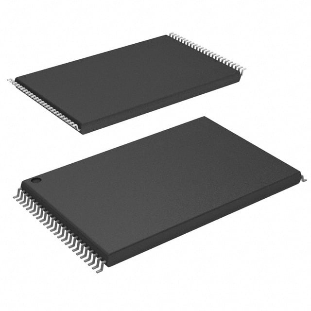
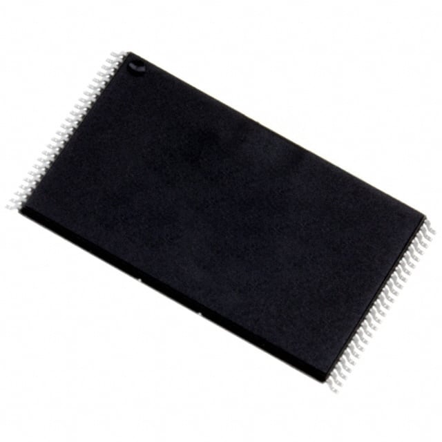
- Package Available in a 48-lead TSOP package (48-TFSOP / 48-TSOP) with a package width of 18.40 mm suitable for board-level, space-conscious applications.
- Operating Temperature Industrial operating range from −40 °C to 85 °C (TA) for use in a wide range of ambient conditions.
- Development & System Support Datasheet references ECC software/hardware models, bad block management and wear-leveling algorithms, and demo/development tools to aid integration and system validation.
Typical Applications
- Mass storage systems Cost-effective NAND storage for devices and modules requiring non-volatile bulk storage and spare-area management.
- Boot and firmware storage Supports automatic page 0 read at power-up and electronic signature features to enable boot-from-NAND and automatic memory download.
- Embedded microcontroller systems Parallel x8 interface and simple chip-enable options permit direct interfacing with microcontrollers for application code and data storage.
- Industrial equipment Operation across −40 °C to 85 °C and hardware data protection during power transitions make the device suitable for industrial embedded storage tasks.
Unique Advantages
- Mid-density NAND in a compact package: 128 Mbit capacity in a 48-TSOP footprint delivers significant non-volatile storage without large PCB area impact.
- Parallel x8 interface with pinout compatibility: Multiplexed address/data and common pinout across densities simplify design migration between capacities.
- Boot and system-download support: Automatic page 0 read at power-up and electronic signature options streamline firmware boot and memory initialization.
- Robust data protection: Program/erase locked during power transitions and documented endurance/retention figures (100,000 cycles; 10 years retention) help maintain data integrity.
- Practical performance profile: Fast sequential access (50 ns) and typical page program/erase timings (page program ~200 μs; block erase ~2 ms) balance throughput and predictable latency for embedded storage tasks.
- Development support included in datasheet: ECC models, bad block management, wear-leveling algorithms and demo tools are referenced to accelerate integration and validation.
Why Choose IC FLASH 128MBIT PARALLEL 48TSOP?
The NAND128W3A0AN6 positions itself as a practical, mid-density NAND flash option for designs that need parallel x8 non-volatile storage with boot support and documented endurance and retention. Its 2.7–3.6 V supply range, industrial temperature rating, hardware data protection and compact 48-TSOP package make it suitable for embedded systems, storage modules, and applications requiring reliable boot/firmware storage.
Engineers designing systems that prioritize straightforward microcontroller interfacing, predictable read/program/erase behavior, and access to ECC and block management resources will find the device aligned with integration and lifecycle needs documented in the product datasheet.
Request a quote or submit an inquiry to receive pricing, lead-time and availability information for the NAND128W3A0AN6 IC FLASH 128MBIT PARALLEL 48TSOP.


Date Founded: 1987
Headquarters: Plan-les-Ouates, Geneva, Switzerland
Employees: 50,000+
Revenue: $17.24 Billion
Certifications and Memberships: ISO9001:2015, ISO14001:2015, ISO45001:2018, IATF16949:2016, ISO50001:2018


