
NAND128W3A0AN6F
| Part Description |
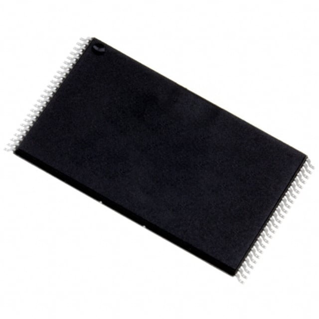
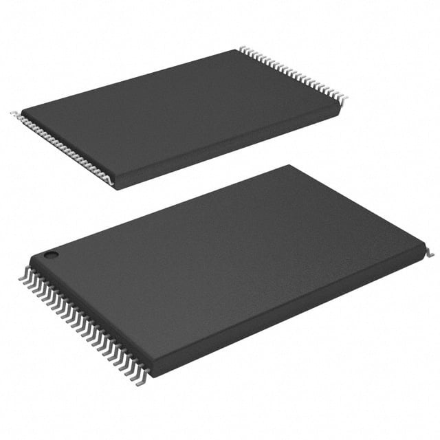
IC FLASH 128MBIT PARALLEL 48TSOP |
|---|---|
| Quantity | 942 Available (as of June 18, 2026) |
| Product Category | Flash Memory |
|---|---|
| Manufacturer | STMicroelectronics |
| Manufacturing Status | Obsolete |
| Manufacturer Standard Lead Time | Contact Us |
| Datasheet |
Specifications & Environmental
| Device Package | 48-TSOP | Memory Format | FLASH | Technology | FLASH - NAND | ||
|---|---|---|---|---|---|---|---|
| Memory Size | 128 Mbit | Access Time | 50 ns | Grade | Industrial | ||
| Clock Frequency | N/A | Voltage | 2.7V ~ 3.6V | Memory Type | Non-Volatile | ||
| Operating Temperature | -40°C ~ 85°C (TA) | Write Cycle Time Word Page | 50 ns | Packaging | 48-TFSOP (0.724", 18.40mm Width) | ||
| Mounting Method | Non-Volatile | Memory Interface | Parallel | Memory Organization | 16M x 8 | ||
| Moisture Sensitivity Level | 3 (168 Hours) | RoHS Compliance | ROHS3 Compliant | REACH Compliance | REACH Unaffected | ||
| Qualification | N/A | ECCN | 3A991B1A | HTS Code | 8542.32.0071 |
Overview of NAND128W3A0AN6F – IC FLASH 128MBIT PARALLEL 48TSOP
The NAND128W3A0AN6F from STMicroelectronics is a 128‑Mbit non‑volatile NAND flash memory organized as 16M × 8 with a parallel (x8) interface. It provides high‑density block and page storage suitable for mass storage and embedded firmware/boot applications that require NAND architecture and page‑oriented operations.
Designed for 3.0V systems (VDD = 2.7 V to 3.6 V) and operating from −40°C to 85°C, the device is offered in a 48‑TSOP package and includes page, block and system features that support fast data movement and reliable program/erase cycles.
Key Features
- Memory Architecture 128 Mbit NAND flash organized as 16M × 8 with a page size of 512 + 16 spare bytes (x8 device).
- Interface Parallel NAND interface with multiplexed address/data signals and x8 bus width for direct connection to parallel controllers.
- Performance Sequential access down to 50 ns, random page read up to 12 μs (max), and typical page program time of 200 μs. Write/read timing supports fast page operations and copy‑back programming.
- Endurance and Data Retention Specified for 100,000 program/erase cycles and 10 years data retention to support long‑lived storage requirements.
- Power 3.0V device operating range: 2.7 V to 3.6 V, suitable for standard 3V system rails.
- Package and Temperature Available in a 48‑TSOP (48‑TFSOP) package (0.724", 18.40 mm width) with an operating temperature range of −40°C to 85°C.
- System and Reliability Features Hardware data protection during power transitions (program/erase locked), automatic page 0 read at power‑up for boot support, and a status register and electronic signature for system management.
Typical Applications
- Mass storage devices High‑density NAND array provides cost‑effective bulk storage for embedded mass storage applications.
- Embedded boot and firmware storage Automatic page‑0 read at power‑up supports boot‑from‑NAND scenarios and system firmware download at startup.
- High‑density non‑volatile storage Suitable for designs that require block and page management, copy‑back programming and spare area for error management and metadata.
Unique Advantages
- High‑density NAND array: 128 Mbit capacity in a compact 48‑TSOP package provides significant storage density for space‑constrained designs.
- Parallel x8 interface: Multiplexed address/data bus and x8 width enable straightforward integration with parallel host controllers.
- Fast page operations: Sequential access to 50 ns, random page read up to 12 μs, and page program ≈200 μs for efficient data throughput and programming cycles.
- Robust endurance and retention: 100,000 program/erase cycles and 10 years retention support durable, long‑term storage use cases.
- Power and thermal compatibility: Operates from 2.7 V to 3.6 V and across −40°C to 85°C, matching common 3V system environments and industrial temperature requirements.
- Boot and system support: Automatic page‑0 read at power‑up and copy‑back program mode simplify boot sequencing and fast internal page transfers without external buffering.
Why Choose NAND128W3A0AN6F?
NAND128W3A0AN6F is positioned as a compact, high‑density NAND flash option for designs that need reliable non‑volatile storage with page‑oriented performance and system‑level features such as automatic power‑up page read and hardware data protection during power transitions. Its endurance and retention specifications make it appropriate for applications requiring sustained program/erase cycling and long‑term data preservation.
This device is suitable for engineers implementing mass storage or embedded boot solutions who require a parallel x8 NAND flash with defined timing characteristics, robust block management capabilities and a 48‑TSOP footprint for PCB integration.
Request a quote or submit a pricing and availability inquiry to receive lead time and ordering information for the NAND128W3A0AN6F.


Date Founded: 1987
Headquarters: Plan-les-Ouates, Geneva, Switzerland
Employees: 50,000+
Revenue: $17.24 Billion
Certifications and Memberships: ISO9001:2015, ISO14001:2015, ISO45001:2018, IATF16949:2016, ISO50001:2018


