TH58NVG5S0FTA20
| Part Description |
IC FLASH 32GBIT PAR 48TSOP I |
|---|---|
| Quantity | 1,320 Available (as of June 15, 2026) |
| Product Category | Memory |
|---|---|
| Manufacturer | Kioxia America, Inc. |
| Manufacturing Status | Active |
| Manufacturer Standard Lead Time | 24 Weeks |
| Datasheet |
Specifications & Environmental
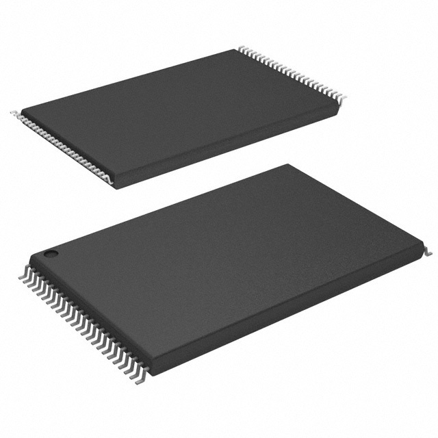
| Device Package | 48-TSOP I | Memory Format | FLASH | Technology | FLASH - NAND (SLC) | ||
|---|---|---|---|---|---|---|---|
| Memory Size | 32 Gbit | Access Time | 25 ns | Grade | Commercial | ||
| Clock Frequency | N/A | Voltage | 2.7V ~ 3.6V | Memory Type | Non-Volatile | ||
| Operating Temperature | 0°C ~ 70°C (TA) | Write Cycle Time Word Page | 25 ns | Packaging | 48-TFSOP (0.724", 18.40mm Width) | ||
| Mounting Method | Non-Volatile | Memory Interface | Parallel | Memory Organization | 4G x 8 | ||
| Moisture Sensitivity Level | 3 (168 Hours) | RoHS Compliance | ROHS3 Compliant | REACH Compliance | REACH Unaffected | ||
| Qualification | N/A | ECCN | 3A991B1A | HTS Code | 8542.32.0071 |
Overview of TH58NVG5S0FTA20 – IC FLASH 32GBIT PAR 48TSOP I
The TH58NVG5S0FTA20 from Kioxia America, Inc. is a 32 Gbit (4G × 8) NAND flash memory device organized for high-density non-volatile storage. It implements CMOS NAND E²PROM architecture with on-chip registers and supports automated program and erase operations.
Engineered for embedded storage uses, the device targets solid-state file storage, voice recording and image-file memory in still cameras and other systems that require large-capacity, non-volatile data retention within a 48‑TSOP I package.
Key Features
- Memory Capacity & Organization — 32 Gbit total capacity organized as 4G × 8; memory array and two 4,328‑byte static registers enable data transfer in 4,328‑byte increments.
- Flash Technology — FLASH - NAND (SLC) technology providing non-volatile storage suitable for repeated program/erase cycles.
- Interface & Mode Control — Parallel x8 organization with serial input/output and command-control modes that use I/O pins for address, data and command inputs.
- Performance — Serial read cycle down to 25 ns (CL=100 pF); cell-array-to-register transfer up to 30 µs maximum; auto page program typically 300 µs/page and auto block erase typically 3 ms/block.
- Power — Single supply operation from 2.7 V to 3.6 V; typical operating currents specified (Read/Program/Erase max 30 mA, Standby max 200 µA).
- Erasure & Program Granularity — Erase implemented per block (256 Kbytes + 14.5 Kbytes: 4,328 bytes × 64 pages); page size 4,328 bytes.
- Reliability & Maintenance — Minimum number of valid blocks specified (min 16,064 blocks); design requires 4‑bit ECC per each 512‑byte sector.
- Package & Temperature — 48‑TSOP I (48‑TFSOP, 0.724" / 18.40 mm width) package; operating temperature range 0°C to 70°C.
Typical Applications
- Solid-State File Storage — High-density NAND storage for embedded file systems requiring large non-volatile capacity and block-level erase/program control.
- Voice Recording Systems — Stores recorded audio data with page/program and block/erase management suited for streaming or chunked writes.
- Still Image Memory — Image-file storage for digital cameras and imaging devices that need large-capacity non-volatile memory in a compact TSOP package.
Unique Advantages
- High Capacity in Compact Package: 32 Gbit NAND in a 48‑TSOP I package reduces board area while providing large non-volatile storage.
- On-Chip Register Architecture: Two 4,328‑byte static registers enable block-wise data transfers between register and cell array for streamlined program/read operations.
- Automated Program/Erase Operations: Auto page program and auto block erase simplify host control and reduce firmware overhead for common memory operations.
- Defined Performance Metrics: Specified read cycle (25 ns), cell-to-register transfer (30 µs max), and typical program/erase times allow predictable system timing and performance planning.
- System-Level ECC Requirement: Explicit 4‑bit ECC per 512‑byte sector requirement supports data integrity planning at the system level.
- Low-Voltage Single-Supply Operation: 2.7 V to 3.6 V supply range matches common 3.3 V embedded platforms for straightforward power integration.
Why Choose TH58NVG5S0FTA20?
The TH58NVG5S0FTA20 provides a clear specification set for high-density NAND storage: 32 Gbit capacity, defined timing for read/program/erase operations, and on-chip registers for efficient data movement. Its 48‑TSOP I footprint and single‑supply 2.7 V–3.6 V operation make it suitable for compact embedded systems requiring robust non-volatile storage within a 0°C to 70°C operating window.
This device is a fit for designers and integrators building products that need block-level erase/program control, predictable performance numbers, and an explicitly stated ECC requirement to support system data integrity planning.
Request a quote or submit an inquiry to sales for availability, pricing and lead‑time information for the TH58NVG5S0FTA20.