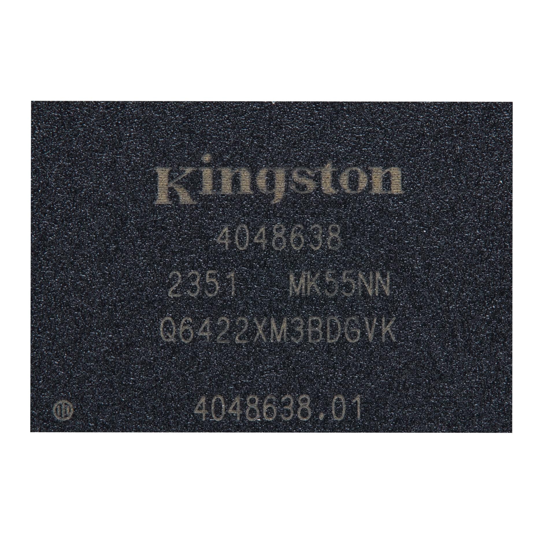
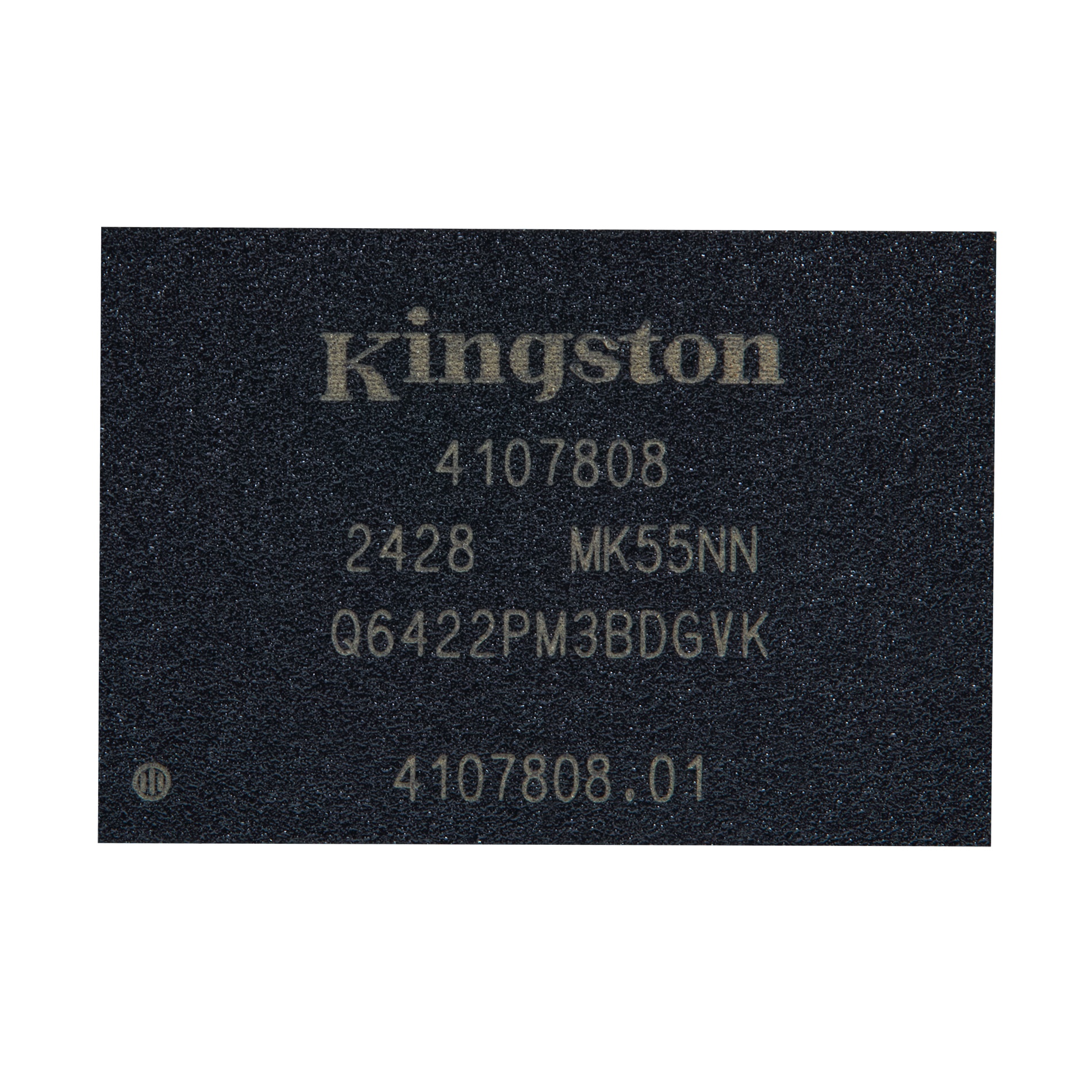
Q6422PM3BDGVK-U
| Part Description |
64GB 200 BALL FBGA LPDDR4 4266MH |
|---|---|
| Quantity | 1,340 Available (as of June 15, 2026) |
| Product Category | Memory |
|---|---|
| Manufacturer | Kingston Technology |
| Manufacturing Status | Active |
| Manufacturer Standard Lead Time | 24 Weeks |
| Datasheet |
Specifications & Environmental
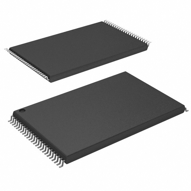
| Device Package | 200-FBGA (10x14.5) | Memory Format | DRAM | Technology | SDRAM - Mobile LPDDR4 | ||
|---|---|---|---|---|---|---|---|
| Memory Size | 64 Gbit | Access Time | 3.5 ns | Grade | Industrial | ||
| Clock Frequency | 2.133 GHz | Voltage | 1.06V ~ 1.17V, 1.7V ~ 1.95V | Memory Type | N/A | ||
| Operating Temperature | -25°C ~ 85°C | Write Cycle Time Word Page | N/A | Packaging | 200-VFBGA | ||
| Mounting Method | N/A | Memory Interface | N/A | Memory Organization | 2G x 16 | ||
| Moisture Sensitivity Level | 3 (168 Hours) | RoHS Compliance | Unknown | REACH Compliance | REACH Unknown | ||
| Qualification | N/A | ECCN | 3A991B2A | HTS Code | 8542.32.0041 |
Overview of Q6422PM3BDGVK-U – 64GB 200 BALL FBGA LPDDR4 4266MH
The Q6422PM3BDGVK-U is a Low Power DRAM (LPDDR4) device supplied in a 200-ball FBGA package. It delivers a 64 Gbit memory configuration implemented as 2048M × 16 I/O × 2 channels with four die per device.
Designed for mobile LPDDR4 applications, the device supports a maximum data rate of 4266 Mbps (clock frequency 2.133 GHz) and low-voltage operation with defined VDD1 and VDD2/VDDCA/VDDQ supply ranges. It targets compact, high-bandwidth memory subsystems that require low power and fine-grained refresh control.
Key Features
- Memory Organization and Density — 64 Gbit total capacity (2048M × 16 × 2 channels), built from four 16 Gbit die; device configuration supports two channels and two ranks for parallel operation.
- High Data Rate — Supports up to 4266 Mbps with a clock frequency of 2.133 GHz; backward compatible with lower frequencies per datasheet limits.
- Low-Power Operation — Dual supply domains: VDD1 = 1.70 V to 1.95 V and VDD2/VDDCA/VDDQ = 1.06 V to 1.17 V to support LPDDR4 power profiles.
- Package — 200-ball FBGA package (200-FBGA, 10 × 14.5 mm) for compact board-level integration.
- Memory Access and Timing — Eight internal banks per channel, programmable read/write latencies (RL/WL), burst lengths 16, 32 and on-the-fly burst mode selectable via MRS.
- Data Integrity and Interface — Differential clock inputs (CK_t/CK_c), bi-directional differential data strobe (DQS_t/DQS_c) and DBI pin support for data masking and DBIdc functionality.
- Refresh and Power Management — Auto-refresh, self-refresh, per-bank refresh, Partial Array Self-Refresh (PASR), bank/segment masking, and Auto Temperature Compensated Self-Refresh (ATCSR) via the integrated temperature sensor. Refresh cycles: 8192 cycles/32 ms (average refresh period 3.9 μs).
- Operating Temperature — Standard operating temperature range TC = −25 °C to +85 °C; industrial temperature range TC = −40 °C to +95 °C is documented in the datasheet.
Typical Applications
- Mobile devices — LPDDR4 architecture and low-voltage operation make this device suitable for memory subsystems in mobile and battery-powered designs requiring high bandwidth and low power.
- Compact embedded systems — 200-ball FBGA package and high-density 64 Gbit capacity support space-constrained modules and embedded memory implementations.
- High-bandwidth compute modules — Dual-channel configuration and eight banks per channel enable concurrent accesses and sustained throughput for performance-focused modules.
Unique Advantages
- High aggregate bandwidth: 4266 Mbps maximum data rate with 2.133 GHz clocking for designs demanding high-throughput memory.
- Scalable density in a compact package: 64 Gbit device built from four 16 Gbit die in a 200-ball FBGA (10 × 14.5 mm) reduces board area while providing large memory capacity.
- Fine-grained power control: Multiple supply domains and LPDDR4 power profile support enable lower overall power consumption in mobile and embedded platforms.
- Robust refresh and power modes: Per-bank refresh, PASR, ATCSR and self-refresh modes provide flexible refresh management to optimize retention and power.
- Flexible timing and driver control: Programmable RL/WL and driver strength allow designers to tune timing and signal integrity for target system configurations.
Why Choose Q6422PM3BDGVK-U?
The Q6422PM3BDGVK-U positions itself as a high-density LPDDR4 memory device delivering 64 Gbit capacity, dual-channel operation and up to 4266 Mbps data throughput in a compact 200-ball FBGA. Its combination of programmable timing, per-bank features and low-voltage operation makes it suitable for mobile and embedded systems where bandwidth, power efficiency and board area are key considerations.
Developers and system integrators requiring a high-capacity, low-power LPDDR4 component can rely on the documented electrical ranges, refresh behavior and interface features to plan integration, thermal management and power sequencing for robust system behavior across the specified temperature ranges.
Request a quote or submit an inquiry to discuss volume pricing, lead times and technical availability for Q6422PM3BDGVK-U.