
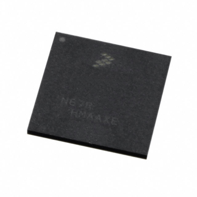
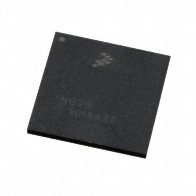
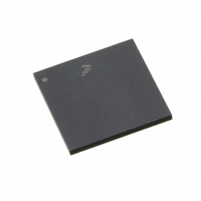
LS1012ASN7EKB
| Part Description |
ARM® Cortex®-A53 Microprocessor IC QorIQ® Layerscape 1 Core, 64-Bit 600MHz 211-FCLGA (9.6x9.6) |
|---|---|
| Quantity | 215 Available (as of October 8, 2026) |

| Product Category | Microprocessors |
|---|---|
| Part Series | LS1012A |
| Manufacturer | NXP USA Inc. |
| Manufacturing Status | Active |
| Manufacturer Standard Lead Time | 18 Weeks |
| Datasheet |
Specifications & Environmental
| Core Processor | ARM® Cortex®-A53 | Device Package | 211-FCLGA (9.6x9.6) | ECCN | 3A991A2 | ||
|---|---|---|---|---|---|---|---|
| Ethernet | GbE (2) | HTS Code | 8542.31.0001 | Moisture Sensitivity Level | 3 (168 Hours) | ||
| Mounting Method | Surface Mount | Mounting Type | Surface Mount | Number of Cores/Bus Width | 1 Core, 64-Bit | ||
| Operating Temperature | 0°C ~ 105°C | Package / Case | 211-VFLGA | RAM Controllers | DDR3L | ||
| REACH Compliance | REACH Unaffected | RoHS Compliance | ROHS3 Compliant | SATA | SATA 6Gbps (1) | ||
| Security Features | Secure Boot, TrustZone® | Speed | 600MHz | Supplier Device Package | 211-FCLGA (9.6×9.6) | ||
| USB | USB 2.0 (1), USB 3.0 + PHY |
Overview of LS1012ASN7EKB – QorIQ Layerscape 1‑Core 64‑Bit 600 MHz Microprocessor
The LS1012ASN7EKB is an NXP QorIQ Layerscape microprocessor featuring a single 64‑bit ARM® Cortex®‑A53 core clocked at 600 MHz in a compact 211‑FCLGA (9.6 × 9.6 mm) package. It targets small form‑factor, fanless networking and embedded storage applications that require balanced compute, low power and integrated I/O.
Designed for connected devices and edge systems, the device pairs compute with hardware packet acceleration and trust‑enabled security features to deliver efficient packet processing and secure boot capability in RoHS‑compliant silicon.
Key Features
- Core ARM® Cortex®‑A53 single core, 64‑bit architecture operating at 600 MHz for general embedded compute.
- Cache and CPU features Includes NEON SIMD and dual‑precision FPU plus ECC‑protected caches as described in the product family documentation to support reliable compute workloads.
- Memory DDR3L memory controller support for low‑voltage DRAM configurations.
- Networking and Storage Interfaces Integrated interfaces include up to two Gigabit Ethernet ports, one SATA 6 Gbps port, a USB 3.0 controller with integrated PHY and a USB 2.0 controller.
- High‑speed SerDes and PCIe Multi‑protocol SerDes supports high‑speed interfaces and a DMA‑controlled PCI Express® Gen2 port (as described in the product family documentation).
- Packet Acceleration Hardware packet forwarding engine (PFE) offloads IP packet processing for higher throughput and lower CPU load; documented family performance includes multi‑Gbps forwarding capability.
- Security Secure Boot and Arm TrustZone® support to enable trust‑enabled designs and protected execution environments.
- Package & Mounting 211‑FCLGA (9.6 × 9.6 mm) surface‑mount package.
- Operating Range & Compliance Operational temperature range 0 °C to 105 °C; RoHS compliant.
Typical Applications
- Trust‑enabled IoT Gateways Secure edge aggregation and protocol bridging using integrated security and packet acceleration.
- Consumer and Mobile NAS Compact network‑attached storage and battery‑powered mobile NAS leveraging SATA 6 Gbps and integrated USB interfaces.
- Entry‑level Broadband Ethernet Gateways Broadband gateway platforms that require dual GbE ports and offloaded packet forwarding for efficient throughput.
- Ethernet Drives and Storage Appliances Networked storage devices that benefit from SATA and PCIe connectivity combined with low power operation.
- Building and Factory Automation Embedded controllers and edge nodes that need a small footprint, trusted boot and wired network connectivity.
Unique Advantages
- Integrated I/O in a small footprint: Dual GbE, SATA 6 Gbps, USB 3.0 with PHY and USB 2.0 consolidate interfaces while preserving a 9.6 × 9.6 mm package.
- Hardware packet offload: The PFE offloads IP packet processing to deliver higher forwarding throughput with minimal CPU load, improving system efficiency.
- Trust and secure boot: Built‑in Secure Boot and TrustZone® support help establish a secure platform foundation for connected devices.
- Low‑power, fanless suitability: Family documentation highlights a ~1 W typical power communications processor profile enabling fanless, small form‑factor designs.
- Robust ecosystem and enablement: Evaluation boards, a Linux BSP and development tool support (as provided for the product family) accelerate prototyping and software bring‑up.
Why Choose LS1012ASN7EKB?
LS1012ASN7EKB positions itself as a compact, integration‑focused processor for embedded networking and storage applications that need secure, efficient packet processing without sacrificing interface options. Its combination of a 64‑bit ARM® Cortex®‑A53 core, hardware packet acceleration, trusted boot mechanisms and multiple high‑speed I/O ports makes it suitable for fanless gateways, NAS devices and other edge appliances.
Backed by the Layerscape product family enablement—evaluation boards, software BSPs and an established ecosystem—this part offers a practical path from evaluation to deployment for developers seeking a small, secure and feature‑rich platform.
Request a quote or submit a procurement inquiry for LS1012ASN7EKB to receive pricing, availability and information about evaluation board options and software enablement.























Date Founded: 2006
Headquarters: Eindhoven, North Brabant, Netherlands
Employees: 38,000+
Revenue: $10.53 Billion
Certifications and Memberships: ISO9001:2015, IATF16949:2016


