
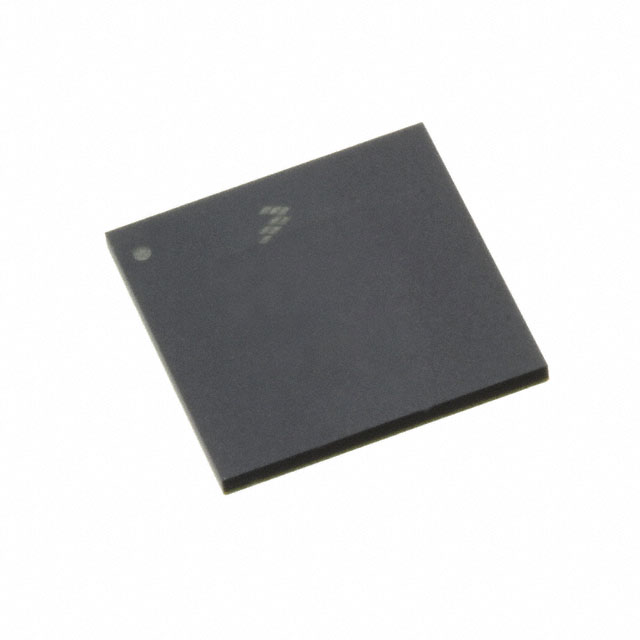
LS1012AXN7HKA
| Part Description |
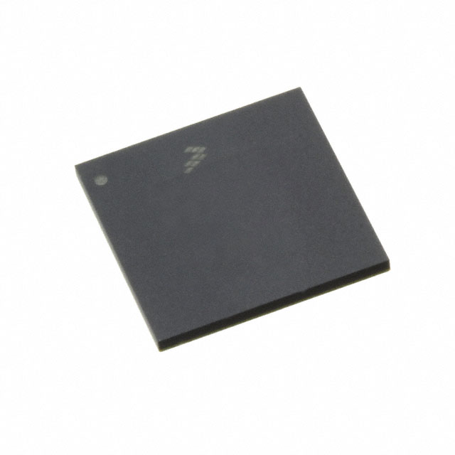
ARM® Cortex®-A53 Microprocessor IC QorIQ® Layerscape 1 Core, 64-Bit 800MHz 211-FCLGA (9.6x9.6) |
|---|---|
| Quantity | 70 Available (as of October 8, 2026) |
| Product Category | Microprocessors |
|---|---|
| Part Series | LS1012A |
| Manufacturer | NXP USA Inc. |
| Manufacturing Status | Active |
| Manufacturer Standard Lead Time | 39 Weeks |
| Datasheet |
Specifications & Environmental
| Core Processor | ARM® Cortex®-A53 | Device Package | 211-FCLGA (9.6x9.6) | ECCN | 3A991A2 | ||
|---|---|---|---|---|---|---|---|
| Ethernet | GbE (2) | HTS Code | 8542.31.0001 | Moisture Sensitivity Level | 3 (168 Hours) | ||
| Mounting Method | Surface Mount | Mounting Type | Surface Mount | Number of Cores/Bus Width | 1 Core, 64-Bit | ||
| Operating Temperature | -40°C ~ 105°C | Package / Case | 211-VFLGA | RAM Controllers | DDR3L | ||
| REACH Compliance | REACH Unaffected | RoHS Compliance | ROHS3 Compliant | SATA | SATA 6Gbps (1) | ||
| Security Features | Secure Boot, TrustZone® | Speed | 800MHz | Supplier Device Package | 211-FCLGA (9.6×9.6) | ||
| USB | USB 2.0 (1), USB 3.0 + PHY |
Overview of LS1012AXN7HKA – IC MPU QORIQ 800MHZ 211FCLGA
The LS1012AXN7HKA is an NXP QorIQ Layerscape microprocessor integrating a single ARM® Cortex®-A53 64‑bit core running at 800 MHz in a compact 211‑FCLGA (9.6 × 9.6 mm) package. It targets fanless, small form‑factor networking and embedded applications that require hardware packet acceleration, integrated security and low typical power consumption.
Designed for industrial environments, the device combines a coherent cache architecture, DDR3L memory support, multiple high‑speed interfaces and dedicated packet and security accelerators to simplify system design for gateways, NAS, storage and automation applications.
Key Features
- Core Single ARM® Cortex®‑A53 64‑bit core at 800 MHz with NEON SIMD and dual‑precision FPU; ECC‑protected L1 and coherent 256 KB L2 cache for reliable code and data execution.
- Performance CoreMark® performance of over 4,000 as published in the product documentation, delivering efficient processing in a low power envelope.
- Memory Integrated DDR3L memory controller supporting 16‑bit DDR3L devices at up to 1 GHz for system memory requirements.
- Networking and Packet Acceleration Two Gigabit Ethernet ports and a hardware Packet Forwarding Engine (PFE) that offloads IP packet processing; PFE capability noted at 2 Gbit/s IP forwarding even with small packets.
- High‑Speed I/O and SerDes Three‑lane, 6 GHz multi‑protocol SerDes enabling interfaces such as DMA‑controlled PCI Express® Gen2 and other high‑speed links.
- Storage and USB One SATA 3.0 (6 Gbps) port and dual USB controllers — one SuperSpeed USB 3.0 with integrated PHY and one USB 2.0 controller — for storage and peripheral expansion.
- Security Integrated Trust architecture with Secure Boot and TrustZone® support plus hardware acceleration for packet processing and security functions.
- System Interfaces Additional supported interfaces include QuadSPI and SD/MMC for flash and removable storage connectivity.
- Package & Temperature 211‑FCLGA (9.6 × 9.6 mm) surface‑mount package qualified for industrial operation from −40 °C to 105 °C.
- Standards & Compliance Device is RoHS compliant and listed with industrial qualification in the product specifications.
Typical Applications
- Trust‑enabled IoT Gateways Secure edge processing and packet acceleration for gateway devices leveraging Secure Boot and TrustZone® protection.
- Consumer and Mobile NAS Compact NAS and battery‑powered mobile storage appliances using SATA 6 Gbps and USB 3.0 for high‑speed data access.
- Entry‑level Ethernet Gateways and Storage Appliances Fanless, small form‑factor gateways and Ethernet drives that benefit from the Packet Forwarding Engine and integrated GbE ports.
- Building and Factory Automation Industrial automation controllers and embedded networking nodes requiring industrial temperature range and reliable memory/cache protection.
Unique Advantages
- Compact, low‑power integration: Single‑core 64‑bit processor and multiple high‑speed I/O in a 9.6 × 9.6 mm package reduce board area while supporting a 1 W typical power profile in small form‑factor designs.
- Hardware packet and security acceleration: Offloads packet processing and cryptographic workloads from the CPU via dedicated accelerators and PFE, improving throughput and lowering CPU load.
- Embedded reliability features: ECC‑protected caches and industrial qualification across −40 °C to 105 °C enhance system robustness for harsh environments.
- Flexible storage and peripheral connectivity: Native SATA 3.0, USB 3.0 with integrated PHY, USB 2.0 and SD/MMC/QuadSPI support enable a wide range of storage and I/O configurations.
- Ready‑to‑develop ecosystem: Availability of evaluation boards and a Linux BSP for rapid prototyping and software bring‑up accelerates time‑to‑market.
Why Choose LS1012AXN7HKA?
The LS1012AXN7HKA positions itself as a tightly integrated, industrial‑rated solution for compact networking and embedded storage designs that require a balance of performance, security and low power. With a Cortex‑A53 core, coherent caches, DDR3L support and dedicated accelerators for packet forwarding and security, it addresses use cases where efficient throughput and reliable operation matter.
This device is well suited to engineers building fanless gateways, NAS devices, embedded storage appliances and automation nodes who need an established software ecosystem and evaluation support to accelerate development and deployment.
Request a quote or submit an inquiry to receive pricing, availability and lead‑time information for the LS1012AXN7HKA.























Date Founded: 2006
Headquarters: Eindhoven, North Brabant, Netherlands
Employees: 38,000+
Revenue: $10.53 Billion
Certifications and Memberships: ISO9001:2015, IATF16949:2016


