
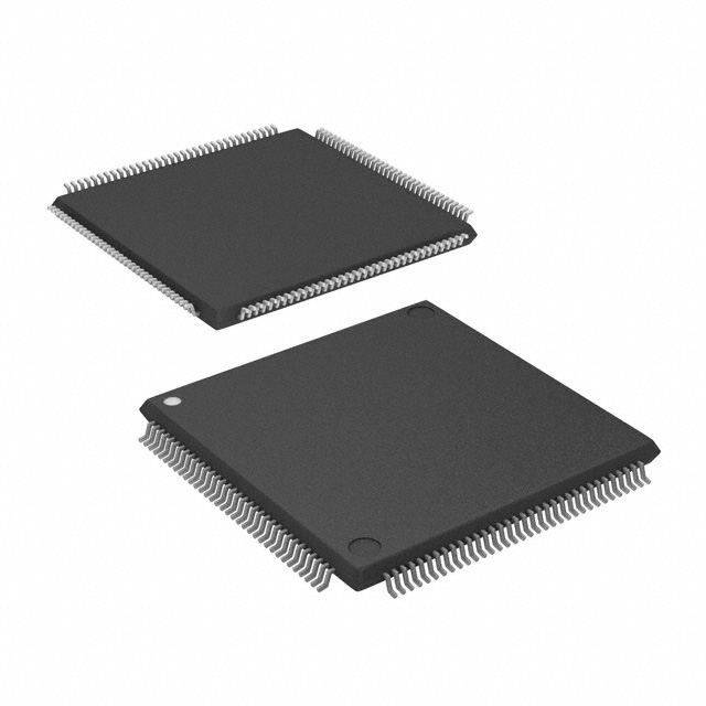
MC68302AG33C
| Part Description |
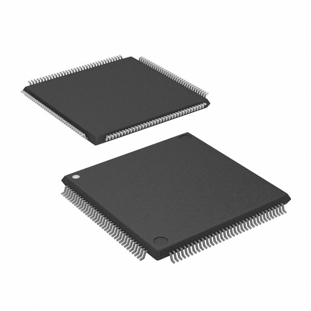
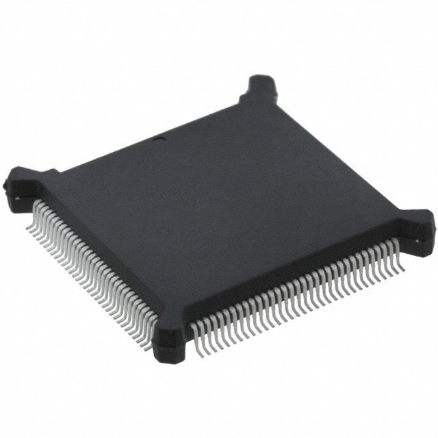
M68000 Microprocessor IC M683xx 1 Core, 8/16-Bit 33MHz 144-LQFP (20x20) |
|---|---|
| Quantity | 521 Available (as of October 8, 2026) |
| Product Category | Microprocessors |
|---|---|
| Part Series | MC68302 |
| Manufacturer | NXP USA Inc. |
| Manufacturing Status | Obsolete |
| Manufacturer Standard Lead Time | Contact Us |
| Datasheet |
Specifications & Environmental
| Co-Processors/DSP | Communications; RISC CPM | Core Processor | M68000 | Device Package | 144-LQFP (20x20) | ||
|---|---|---|---|---|---|---|---|
| ECCN | 3A991A2 | Graphics Acceleration | No | HTS Code | 8542.31.0001 | ||
| Moisture Sensitivity Level | 3 (168 Hours) | Mounting Method | Surface Mount | Mounting Type | Surface Mount | ||
| Number of Cores/Bus Width | 1 Core, 8/16-Bit | Operating Temperature | 0°C ~ 70°C (TA) | Package / Case | 144-LQFP | ||
| RAM Controllers | DRAM | REACH Compliance | REACH Unaffected | RoHS Compliance | ROHS3 Compliant | ||
| Speed | 33MHz | Supplier Device Package | 144-LQFP (20×20) | Voltage – I/O | 5.0V |
Overview of MC68302AG33C – IC MPU M683XX 33MHZ 144LQFP
The MC68302AG33C is an M68000-core microprocessor IC designed for embedded systems. It features a single M68000 core with an 8/16-bit bus implementation and a rated operating frequency of 33 MHz.
Built with integrated communications co-processing and DRAM controller support, the device targets embedded applications that require a compact, surface-mount MPU in a 144-LQFP (20x20) package while operating from a 5 V IO supply within a 0 °C to 70 °C range.
Key Features
- Core & Performance Single M68000 core with an 8/16-bit bus and a clock rate of 33 MHz; timing is characterized at 33 MHz with a cycle period (tcyc) of 30 ns and clock pulse widths (tcl, tch) of 15 ns.
- Co-Processing & Communications Includes communications-focused co-processors and a RISC CPM to assist system-level communications tasks and offload specific processing functions.
- Memory Interface Integrated DRAM controller(s) to support external dynamic memory configurations for system-level data buffering and code storage.
- Interfaces Additional interface support includes GCI for system connectivity and control.
- Power & IO Operates with a 5 V IO voltage, suitable for designs standardized on 5 V signaling.
- Package & Mounting Supplied in a 144-LQFP package (20x20), optimized for surface-mount assembly and compact board-level integration.
- Deterministic Timing Comprehensive timing parameters are provided for 33 MHz operation (examples: 30 ns cycle period, 15 ns clock pulse width, and documented address/data and control timing windows), enabling predictable interface and bus design.
- Environmental Compliance RoHS compliant, supporting regulatory-driven material requirements for electronics manufacturing.
- Operating Range Rated for operation from 0 °C to 70 °C, suitable for commercial-temperature embedded deployments.
Typical Applications
- Embedded Communications Controllers — Use the integrated communications co-processor and CPM to implement protocol handling and interface tasks in embedded communication products.
- Board-Level MPU Solutions — Serve as the main microprocessor in M68000-based board designs where a 33 MHz single-core MPU with DRAM support is required.
- DRAM-Based Embedded Systems — Leverage on-chip DRAM controller support for applications that require external dynamic memory for code and data storage.
Unique Advantages
- Integrated Communications Co-Processing: Reduces external component count by providing communications and RISC CPM support on-chip, simplifying board design for protocol-heavy applications.
- Deterministic Timing at 33 MHz: Timing characterized at 33 MHz (30 ns cycle period and defined clock/data windows) helps designers validate bus and peripheral timing accurately.
- Compact, Surface-Mount Packaging: 144-LQFP (20x20) package supports high-density PCB layouts and standard surface-mount assembly processes.
- DRAM Controller Integration: On-chip DRAM controller capability streamlines memory subsystem design and reduces external glue logic.
- Commercial Temperature Range: Rated 0 °C to 70 °C to match a wide range of embedded product environments.
- Regulatory Compliance: RoHS compliant to meet common material and environmental requirements for modern electronics manufacturing.
Why Choose MC68302AG33C?
The MC68302AG33C combines an M68000 single-core architecture with integrated communications co-processing and DRAM controller support, providing a focused solution for embedded designs that need a 33 MHz MPU in a compact 144-LQFP surface-mount package. Its documented timing at 33 MHz and standardized 5 V IO make it straightforward to integrate into existing M68000-based system designs.
This part is suited to designers and procurement teams building commercial-temperature embedded products that require predictable timing, on-chip communications capabilities, and compliance with RoHS material standards.
Request a quote or submit a purchase inquiry to obtain pricing, availability, and lead-time information for MC68302AG33C. Include your required quantities and any delivery or documentation needs to expedite the response.






















Date Founded: 2006
Headquarters: Eindhoven, North Brabant, Netherlands
Employees: 38,000+
Revenue: $10.53 Billion
Certifications and Memberships: ISO9001:2015, IATF16949:2016


