
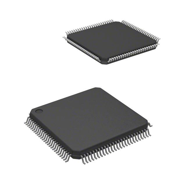
MC68LC302CAF16CT
| Part Description |
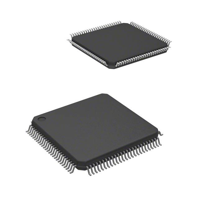
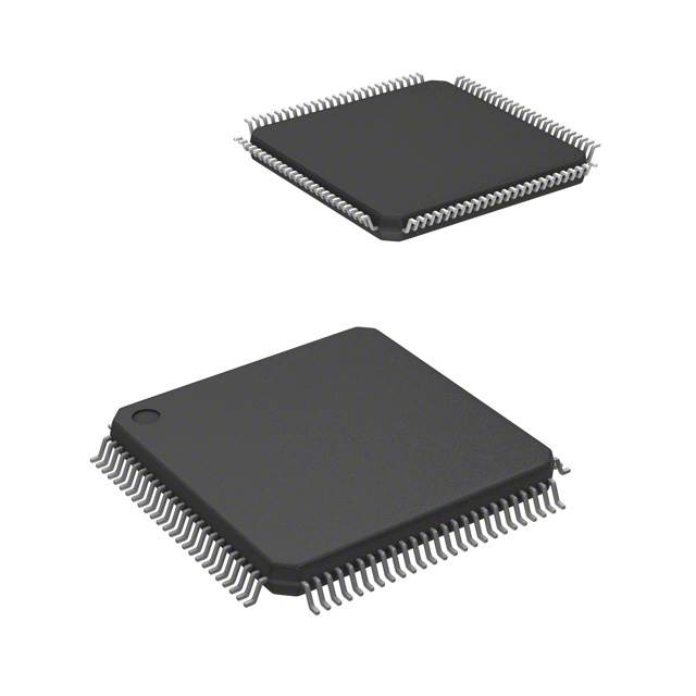
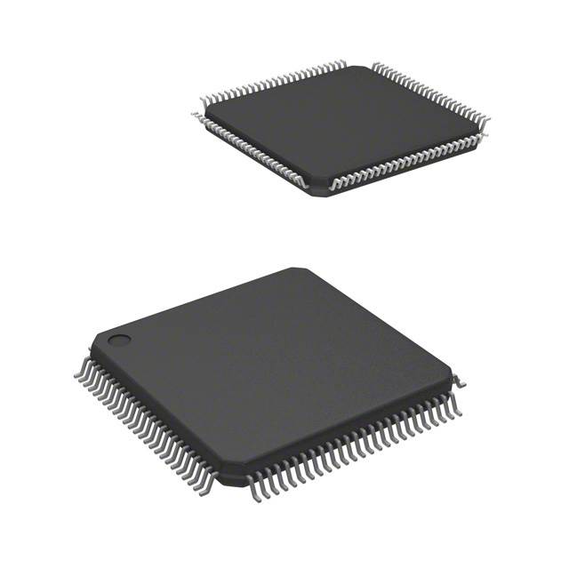
M68000 Microprocessor IC M683xx 1 Core, 8/16-Bit 16MHz 100-LQFP (14x14) |
|---|---|
| Quantity | 391 Available (as of October 8, 2026) |
| Product Category | Microprocessors |
|---|---|
| Part Series | MC68LC302 |
| Manufacturer | NXP USA Inc. |
| Manufacturing Status | Obsolete |
| Manufacturer Standard Lead Time | Contact Us |
| Datasheet |
Specifications & Environmental
| Co-Processors/DSP | Communications; RISC CPM | Core Processor | M68000 | Device Package | 100-LQFP (14x14) | ||
|---|---|---|---|---|---|---|---|
| ECCN | 3A991A2 | Graphics Acceleration | No | HTS Code | 8542.31.0001 | ||
| Moisture Sensitivity Level | 3 (168 Hours) | Mounting Method | Surface Mount | Mounting Type | Surface Mount | ||
| Number of Cores/Bus Width | 1 Core, 8/16-Bit | Operating Temperature | -40°C ~ 85°C (TA) | Package / Case | 100-LQFP | ||
| RAM Controllers | DRAM | REACH Compliance | REACH Unaffected | RoHS Compliance | ROHS3 Compliant | ||
| Speed | 16MHz | Supplier Device Package | 100-LQFP (14×14) | Voltage – I/O | 5.0V |
Overview of MC68LC302CAF16CT – IC MPU M683XX 16MHZ 100LQFP
The MC68LC302CAF16CT is an integrated multiprotocol microprocessor in the MC68LC302 series from NXP Semiconductors. It features an on‑chip static M68000 core with 8/16‑bit system support and a 16 MHz operating speed, combining CPU, memory and communications peripherals in a compact package.
Designed for embedded and industrial applications, this device targets multiprotocol communications, low‑power and space‑constrained systems. Key value comes from its integration of DMA, timers, serial controllers, dual‑port RAM and on‑chip clock/PLL and low‑power modes, enabling simplified board design and reduced external component count.
Key Features
- Core — On‑chip static M68000 core supporting 8‑ or 16‑bit M68000 family system operation at 16 MHz.
- Memory and Bus — On‑chip 1152‑byte dual‑port RAM with programmable address mapping and a system bus supporting 20‑bit addressing and 8/16‑bit data paths; glueless interface to EPROM, SRAM, Flash EPROM and EEPROM.
- Peripherals and Communications — Integrated IDMA controller, interrupt controller, parallel I/O ports and a communications processor (CP) with two full‑duplex serial communications controllers (SCCs) supporting HDLC/SDLC, UART and BISYNC protocols; additional GCI interface.
- Timers and Watchdog — Three timers including a watchdog timer and a Periodic Interrupt Timer (PIT) for real‑time control and system supervision.
- Clock and Low‑Power — On‑chip clock generator and PLL supporting operation with 32 kHz or 4 MHz crystals, plus low‑power standby modes with wake‑up sources and freeze control for debugging.
- Memory Controller — On‑chip DRAM refresh controller and support for external DRAM.
- Package and Environmental — 100‑LQFP (14 × 14 mm) surface‑mount package; industrial operating temperature range −40 °C to 85 °C; RoHS compliant; 5 V I/O.
Typical Applications
- Embedded Communications — Multiprotocol network equipment and serial communications modules leveraging on‑chip SCCs and DMA for protocol handling.
- Portable and Low‑Power Devices — Battery‑sensitive or power‑constrained systems benefiting from the device’s low‑power modes and integrated clock/PLL options.
- Height‑Restricted Systems (PCMCIA) — Compact 100‑LQFP package suitable for space‑ and height‑limited applications such as PCMCIA form‑factor designs.
- Industrial Control — Controllers and monitoring equipment that require industrial temperature qualification, watchdog supervision and multiple timers.
Unique Advantages
- Highly integrated multiprotocol design: Combines CPU, DMA, dual‑port RAM, serial controllers and timers to reduce external components and simplify system architecture.
- Flexible clocking and low‑power options: On‑chip PLL and clock generator plus standby modes allow power‑optimized designs and flexible crystal choices.
- Compact surface‑mount package: 100‑LQFP (14 × 14 mm) reduces PCB area and fits height‑restricted applications.
- Industrial temperature qualification: Rated for −40 °C to 85 °C operation for deployment in industrial environments.
- Direct memory and peripheral support: On‑chip DRAM controller, programmable chip‑selects and glueless external memory interface for straightforward memory integration.
- Proven family architecture: Part of the MC68LC302 series from NXP Semiconductors, providing a consistent feature set for embedded multiprotocol designs.
Why Choose MC68LC302CAF16CT?
The MC68LC302CAF16CT delivers a balanced combination of processing, communications and system integration in a single 100‑LQFP device. With an on‑chip M68000 core, DMA, dual‑port RAM, serial controllers and robust clocking and low‑power capabilities, it is well suited to embedded designs that require a compact, integrated multiprotocol processor operating over an industrial temperature range.
Engineers and procurement teams looking to simplify BOM, save board space and rely on industry‑level temperature performance will find the MC68LC302CAF16CT a practical choice, backed by the MC68LC302 product family from NXP Semiconductors.
Request a quote or submit an inquiry to receive pricing and availability information for the MC68LC302CAF16CT.





















Date Founded: 2006
Headquarters: Eindhoven, North Brabant, Netherlands
Employees: 38,000+
Revenue: $10.53 Billion
Certifications and Memberships: ISO9001:2015, IATF16949:2016


