
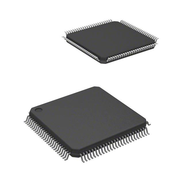
MC68LC302AF16VCT
| Part Description |
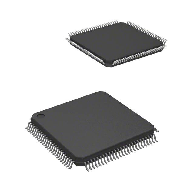
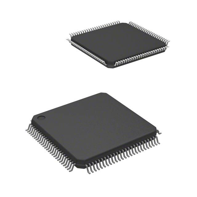
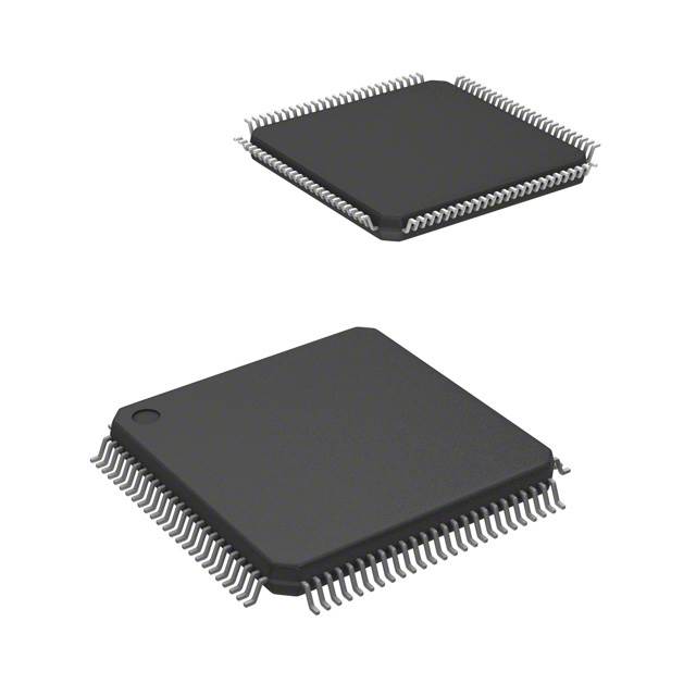
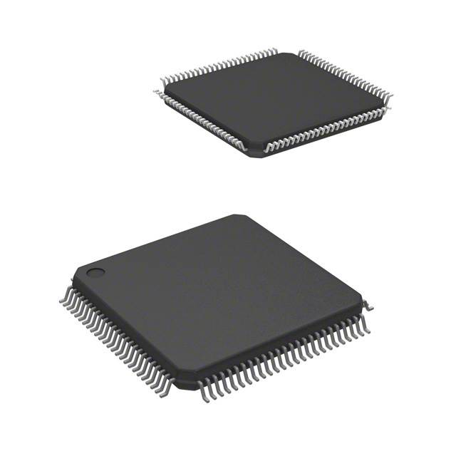
M68000 Microprocessor IC M683xx 1 Core, 8/16-Bit 16MHz 100-LQFP (14x14) |
|---|---|
| Quantity | 553 Available (as of October 8, 2026) |
| Product Category | Microprocessors |
|---|---|
| Part Series | MC68LC302 |
| Manufacturer | NXP USA Inc. |
| Manufacturing Status | Obsolete |
| Manufacturer Standard Lead Time | Contact Us |
| Datasheet |
Specifications & Environmental
| Co-Processors/DSP | Communications; RISC CPM | Core Processor | M68000 | Device Package | 100-LQFP (14x14) | ||
|---|---|---|---|---|---|---|---|
| ECCN | 3A991A2 | Graphics Acceleration | No | HTS Code | 8542.31.0001 | ||
| Moisture Sensitivity Level | 3 (168 Hours) | Mounting Method | Surface Mount | Mounting Type | Surface Mount | ||
| Number of Cores/Bus Width | 1 Core, 8/16-Bit | Operating Temperature | 0°C ~ 70°C (TA) | Package / Case | 100-LQFP | ||
| RAM Controllers | DRAM | REACH Compliance | REACH Unaffected | RoHS Compliance | ROHS3 Compliant | ||
| Speed | 16MHz | Supplier Device Package | 100-LQFP (14×14) | Voltage – I/O | 3.3V |
Overview of MC68LC302AF16VCT – IC MPU M683XX 16MHZ 100LQFP
The MC68LC302AF16VCT is an integrated multiprotocol microprocessor from NXP Semiconductors based on a static M68000 core. It provides a single 8/16-bit M68000-family core running at 16 MHz with on-chip communications and system peripherals targeted at embedded applications.
Designed for compact, low-power embedded systems, the device combines processor, DMA, timers, on-chip dual-port RAM and communications controllers in a 100‑LQFP (14×14 mm) surface-mount package, delivering a space-efficient building block for multiprotocol and portable designs.
Key Features
- Core Static M68000 core supporting 8- or 16-bit system operation at 16 MHz, providing compatibility with M68000-family system designs.
- Memory On-chip 1152‑byte dual-port RAM and support for DRAM controllers; programmable address mapping for on-chip RAM and IMP registers.
- Interfaces & Communications Integrated communications processing resources including a RISC CPM co-processor and two full‑duplex serial communications controllers (SCCs) supporting HDLC/SDLC, UART and BISYNC modes as described in the product family documentation.
- DMA and Bus Independent DMA (IDMA) controller and a general-purpose DMA channel for efficient data movement; four programmable chip-select lines with wait-state generator for glueless interfacing to EPROM, SRAM, Flash and EEPROM.
- Timers & Watchdog Three on-chip timers including a watchdog timer and a periodic interrupt timer (PIT) for system timing and reliability functions.
- System Control & I/O Interrupt controller with selectable modes, parallel I/O ports (some with interrupt capability), system status/control logic and options for low-power standby modes and hardware watchdog control.
- Clocking & Boot On-chip clock generator and PLL supporting operation with 32 kHz or 4 MHz crystals; supports boot in 8-bit mode with the ability to switch to 16-bit operation.
- Electrical & Packaging 3.3 V I/O voltage, surface-mount 100‑LQFP (14×14 mm) package, and an operating temperature range of 0 °C to 70 °C.
Typical Applications
- Embedded Multiprotocol Communications Integrated SCCs and CPM support HDLC/SDLC, UART and BISYNC modes for communications modules and protocol gateways.
- Portable/Low‑Power Devices Low-power standby modes, on-chip clocking and a low-profile 100‑LQFP package make the device suitable for height-restricted and battery‑sensitive designs.
- Compact System Controllers On-chip DMA, timers, PIO and dual‑port RAM enable compact controller designs for embedded appliances and subsystems.
- Memory‑Mapped Embedded Designs Glueless interface to EPROM, SRAM, Flash and EEPROM plus programmable chip-selects simplify external memory integration and boot configurations.
Unique Advantages
- Highly integrated solution: Combines a static M68000 core, DMA, dual‑port RAM and communications controllers on-chip to reduce BOM and board complexity.
- Space-efficient package: 100‑LQFP (14×14 mm) surface-mount package reduces PCB area and supports height-restricted applications.
- Flexible bus operation: Supports 8‑bit boot and run‑time switch to 16‑bit operation for compatibility with a range of memory and system configurations.
- Rich timing and reliability features: Includes three timers, a watchdog timer and a periodic interrupt timer to support robust system supervision and scheduling.
- On-chip clocking and PLL: Built‑in clock generator and PLL support crystal options for simplified clock design and stable system timing.
- Glueless external memory interface: Programmable chip-selects and wait-state logic allow direct connection to common nonvolatile and volatile memories without complex bus glue logic.
Why Choose MC68LC302AF16VCT?
The MC68LC302AF16VCT positions itself as a compact, integrated microprocessor solution for embedded systems that require on-chip communications, DMA, timers and dual‑port RAM alongside a proven M68000-family core. Its combination of integrated peripherals, flexible bus modes and low-profile 100‑LQFP package makes it well suited for designers targeting multiprotocol communications modules, portable devices, and space-constrained embedded controllers.
Backed by NXP Semiconductors' MC68LC302 family documentation and on-chip features such as low‑power modes, PLL clocking and glueless memory interfacing, the device offers a practical platform for reducing external components while retaining system-level functionality.
Request a quote or contact sales to discuss availability, pricing and how the MC68LC302AF16VCT can fit into your next embedded design.





















Date Founded: 2006
Headquarters: Eindhoven, North Brabant, Netherlands
Employees: 38,000+
Revenue: $10.53 Billion
Certifications and Memberships: ISO9001:2015, IATF16949:2016


