
MC68LC302AF20VCT
| Part Description |
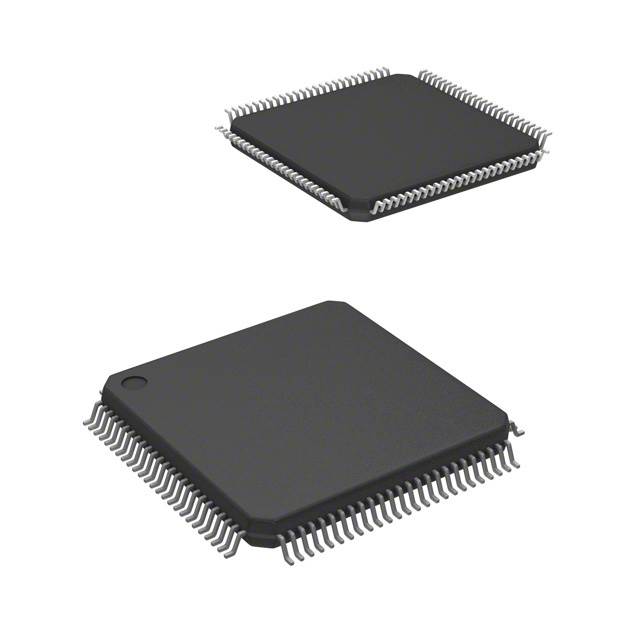
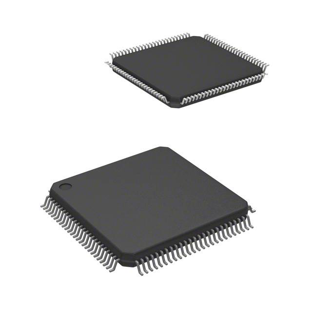
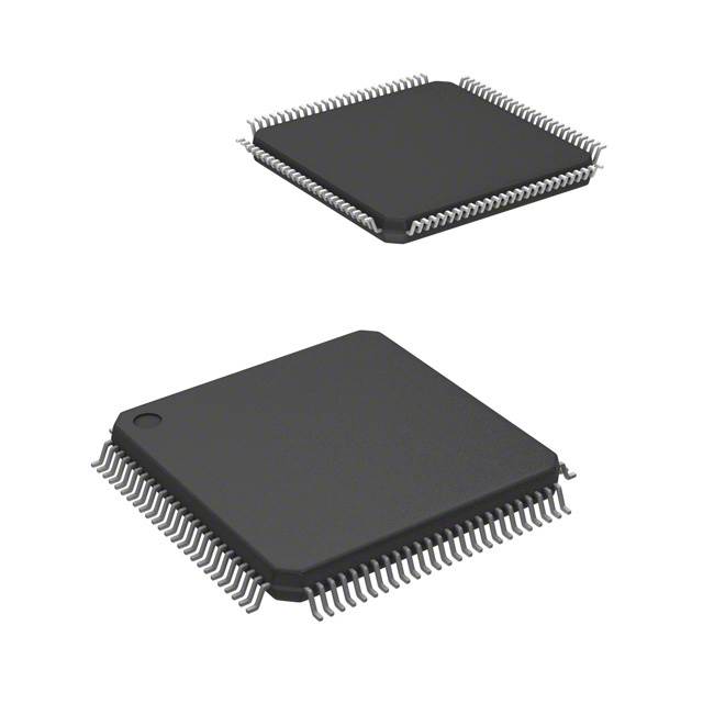
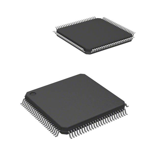
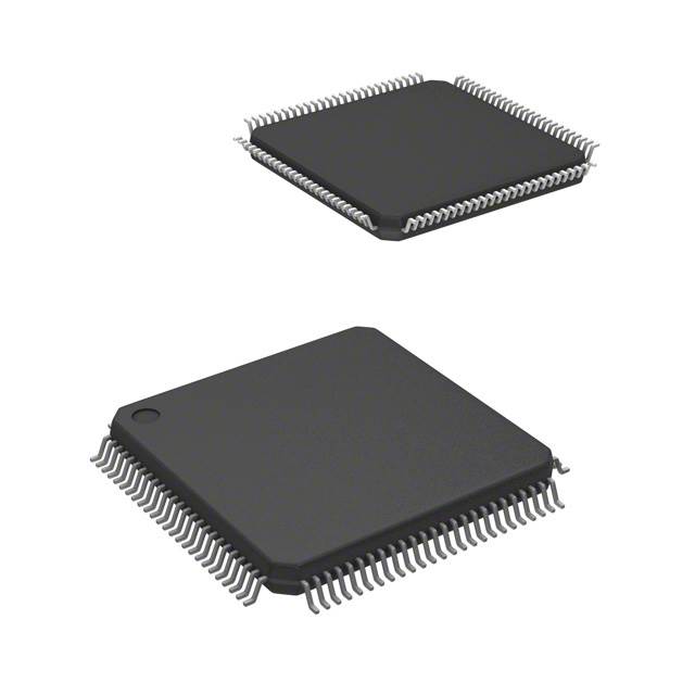
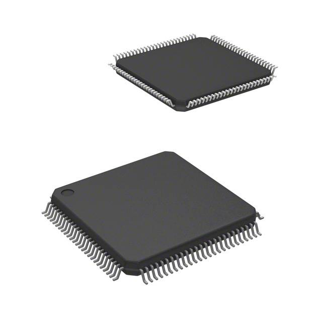
M68000 Microprocessor IC M683xx 1 Core, 8/16-Bit 20MHz 100-LQFP (14x14) |
|---|---|
| Quantity | 275 Available (as of October 8, 2026) |
| Product Category | Microprocessors |
|---|---|
| Part Series | MC68LC302 |
| Manufacturer | NXP USA Inc. |
| Manufacturing Status | Obsolete |
| Manufacturer Standard Lead Time | Contact Us |
| Datasheet |
Specifications & Environmental
| Co-Processors/DSP | Communications; RISC CPM | Core Processor | M68000 | Device Package | 100-LQFP (14x14) | ||
|---|---|---|---|---|---|---|---|
| ECCN | 3A991A2 | Graphics Acceleration | No | HTS Code | 8542.31.0001 | ||
| Moisture Sensitivity Level | 3 (168 Hours) | Mounting Method | Surface Mount | Mounting Type | Surface Mount | ||
| Number of Cores/Bus Width | 1 Core, 8/16-Bit | Operating Temperature | 0°C ~ 70°C (TA) | Package / Case | 100-LQFP | ||
| RAM Controllers | DRAM | REACH Compliance | REACH Unaffected | RoHS Compliance | ROHS3 Compliant | ||
| Speed | 20MHz | Supplier Device Package | 100-LQFP (14×14) | Voltage – I/O | 3.3V |
Overview of MC68LC302AF20VCT – IC MPU M683XX 20MHZ 100LQFP
The MC68LC302AF20VCT is an integrated multiprotocol microprocessor from NXP Semiconductors built around a static M68000 core. Designed for embedded applications, it combines a 20 MHz M68000 CPU with on-chip peripheral controllers and memory to simplify system design for communication and low-power embedded markets.
With integrated DMA, serial controllers and on-chip dual-port RAM, the MC68LC302 series targets compact, height-restricted and portable designs where board space, integration and deterministic peripheral handling are important.
Key Features
- Core & Architecture Static M68000 core supporting 8- or 16-bit system operation and a 20 MHz CPU clock for deterministic embedded processing.
- Memory & On‑Chip RAM Includes 1,152 bytes of on-chip dual-port RAM and support for external DRAM via an on-chip DRAM refresh/controller for shared-memory and buffering needs.
- Communications & Co‑processing Integrated communications processor (RISC CPM) with two independent full-duplex Serial Communications Controllers (SCCs) providing HDLC/SDLC, UART and BISYNC protocol support.
- DMA & Interrupts Independent DMA controller (IDMA) and general-purpose DMA channels combined with an interrupt controller offering two operating modes for flexible real-time event handling.
- Timers & Watchdog Three on-chip timers, including a watchdog timer and a Periodic Interrupt Timer (PIT) for system supervision and periodic tasks.
- System Control & Boot Flexibility On-chip clock generator and PLL (supports 32 kHz or 4 MHz crystals), programmable address mapping, four programmable chip-selects with wait-state logic, and glueless interface to EPROM/SRAM/Flash/EEPROM; supports boot in 8-bit mode with run-time switch to 16-bit mode.
- Low‑Power & Power Management New low-power standby modes with wake-up from dedicated pins and freeze control for debug support.
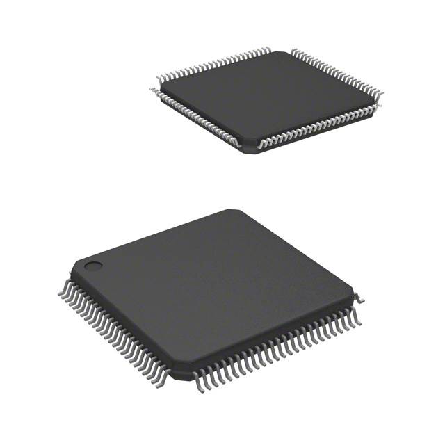
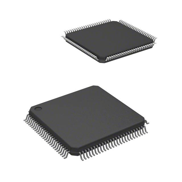
- Package & Environmental Surface-mount 100-LQFP (14 × 14 mm) package, operating temperature range 0 °C to 70 °C, and RoHS compliant.
- Voltage & Interfaces 3.3 V I/O and additional interface support (GCI) for system integration.
Typical Applications
- Embedded Communication Equipment Use the integrated CPM and two SCCs for protocol handling and serial data paths in communication modules and network appliances.
- Portable & Height‑Restricted Devices Low-profile 100-LQFP packaging and low-power modes suit portable designs and PCMCIA-style or other height-restricted form factors.
- Industrial Control & Instrumentation Deterministic timers, watchdog and DMA support make it suitable for real-time control, data acquisition and instrument front-ends.
- Boot/Memory‑Mapped Embedded Systems Glueless external memory interface and programmable chip-selects enable compact systems that boot from various non-volatile memories and transition between 8- and 16-bit operation.
Unique Advantages
- Highly integrated multiprotocol processing: Combines a static M68000 core with a RISC communications processor and two SCCs to reduce board-level components.
- Shared on‑chip RAM: 1,152‑byte dual‑port RAM facilitates low-latency data exchange between CPU and communications engines.
- Flexible memory interfacing: Four programmable chip-selects with wait-state logic and a glueless interface simplify external EPROM/SRAM/Flash/EEPROM integration.
- Built-in timing and supervision: Multiple timers including PIT and watchdog provide reliable task scheduling and system monitoring.
- Space- and power‑efficient package: 100‑LQFP (14×14 mm) surface-mount package and low-power standby modes enable compact, battery-aware designs.
- Standards-focused serial protocols: SCC support for HDLC/SDLC, UART and BISYNC provides protocol flexibility for communication-centric applications.
Why Choose MC68LC302AF20VCT?
The MC68LC302AF20VCT positions itself as a compact, integrated multiprotocol processor ideal for embedded designs requiring on-chip communications, DMA, timers and dual-port RAM around a static M68000 core. Its combination of on-chip peripherals and flexible memory interfaces reduces BOM complexity and board space while providing deterministic control for communication and control applications.
As part of the MC68LC302 series from NXP Semiconductors, this device is suited to designers building portable, height-restricted or communication-focused systems who need a 20 MHz, 3.3 V I/O, surface-mount solution with on-chip resources and low-power options.
Request a quote or submit an inquiry to receive pricing and availability information for the MC68LC302AF20VCT and to discuss fit for your application.





















Date Founded: 2006
Headquarters: Eindhoven, North Brabant, Netherlands
Employees: 38,000+
Revenue: $10.53 Billion
Certifications and Memberships: ISO9001:2015, IATF16949:2016


