
MCIMX255AJM4A
| Part Description |
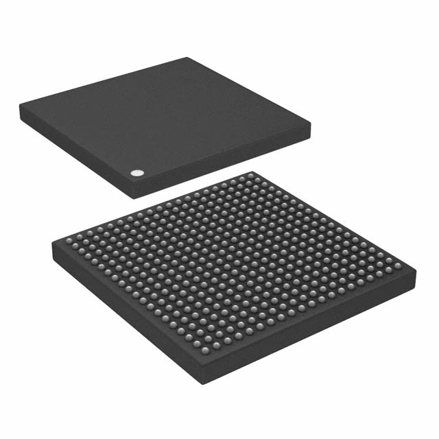
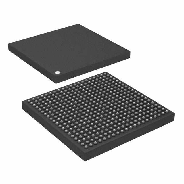
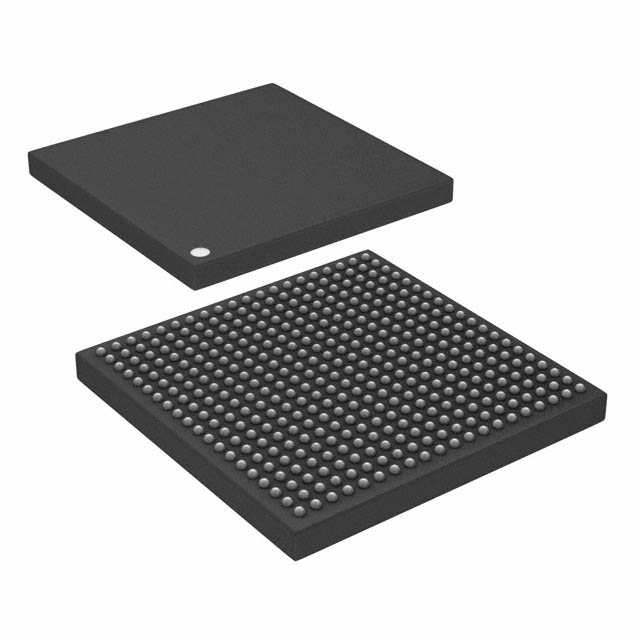
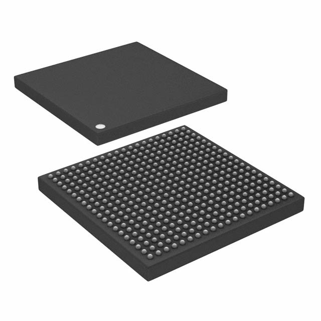
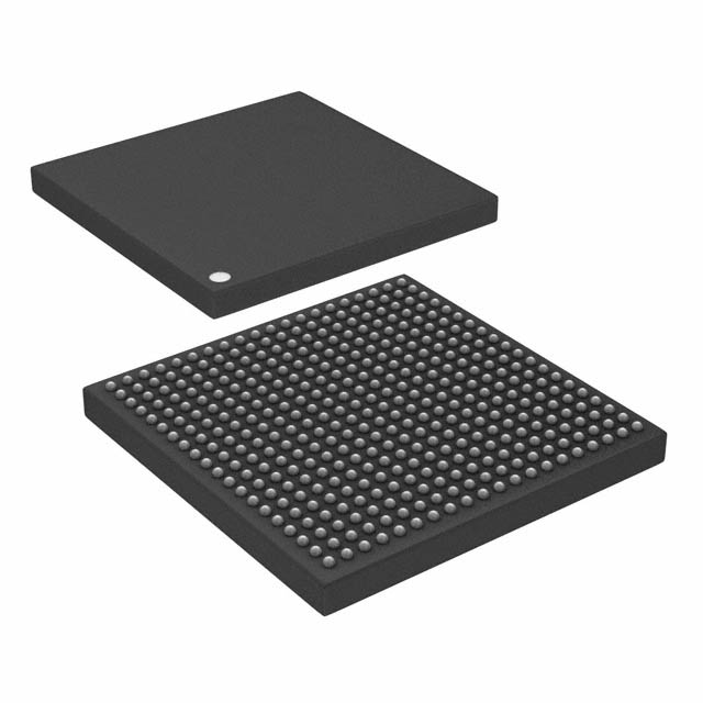
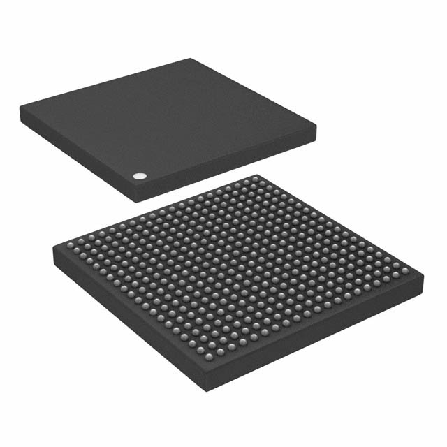
ARM926EJ-S Microprocessor IC i.MX25 1 Core, 32-Bit 400MHz 400-LFBGA (17x17) |
|---|---|
| Quantity | 1,274 Available (as of October 8, 2026) |
| Product Category | Microprocessors |
|---|---|
| Part Series | i.MX 255 |
| Manufacturer | NXP USA Inc. |
| Manufacturing Status | Active |
| Manufacturer Standard Lead Time | 13 Weeks |
| Datasheet |
Specifications & Environmental
| Core Processor | ARM926EJ-S | Device Package | 400-LFBGA (17x17) | Display & Interface Controllers | Keypad, LCD, Touchscreen | ||
|---|---|---|---|---|---|---|---|
| ECCN | 5A992C | Ethernet | 10/100Mbps (1) | Graphics Acceleration | No | ||
| HTS Code | 8542.31.0001 | Moisture Sensitivity Level | 3 (168 Hours) | Mounting Method | Surface Mount | ||
| Mounting Type | Surface Mount | Number of Cores/Bus Width | 1 Core, 32-Bit | Operating Temperature | -40°C ~ 85°C (TA) | ||
| Package / Case | 400-LFBGA | RAM Controllers | LPDDR, DDR, DDR2 | REACH Compliance | REACH Unaffected | ||
| RoHS Compliance | ROHS3 Compliant | Security Features | Boot Security, Cryptography, Secure Fusebox, Secure JTAG, Secure Memory, Tamper Detection | Speed | 400MHz | ||
| Supplier Device Package | 400-LFBGA (17×17) | USB | USB 2.0 + PHY (2) | Voltage – I/O | 2.0V, 2.5V, 2.7V, 3.0V, 3.3V |
Overview of MCIMX255AJM4A – IC MPU I.MX25 400MHZ 400LFBGA
The MCIMX255AJM4A is an NXP Semiconductors i.MX 255 series microprocessor featuring a single ARM926EJ-S 32‑bit core running at 400 MHz in a 400‑LFBGA (17×17) package. It integrates a range of memory controller options, multiple I/O interfaces and hardware security features tailored for industrial and IoT‑oriented embedded designs.
With integrated USB 2.0 PHYs, 10/100 Mbps Ethernet, and peripherals for display and control, the device targets embedded systems that require mid‑range processing, secure boot and cryptographic capabilities within an industrial temperature window.
Key Features
- Core ARM926EJ‑S single core, 32‑bit architecture running at 400 MHz for deterministic embedded processing.
- Memory Controllers Supports LPDDR, DDR and DDR2 memory controllers to accommodate a range of system memory configurations.
- Connectivity Integrated 10/100 Mbps Ethernet controller (1) plus dual USB 2.0 interfaces with PHYs for wired network and host/device connectivity.
- Display & Human Interface Controllers for LCD, keypad and touchscreen interfaces to support HMI and operator panels.
- Additional Interfaces CAN interface for industrial field‑bus integration and other serial control needs.
- Security Features On‑chip Boot Security, Cryptography, Secure Fusebox, Secure JTAG, Secure Memory and Tamper Detection for layered device protection.
- Package & Mounting 400‑LFBGA (17×17) surface‑mount package suitable for compact embedded board designs.
- Operating Range Industrial temperature range of −40°C to 85°C for deployment in demanding environments.
- Environmental Compliance RoHS compliant construction.
Typical Applications
- Industrial HMI and control panels Leverages LCD, touchscreen and keypad controllers plus industrial temperature rating for operator interfaces and local control stations.
- IoT gateways and edge devices Ethernet and USB PHYs combined with onboard security features support networked edge processing and secure device provisioning.
- Embedded control modules ARM926EJ‑S processing with DDR/LPDDR memory support and CAN interface enables machine control, sensor aggregation and real‑time supervisory tasks.
Unique Advantages
- Balanced processing performance: ARM926EJ‑S at 400 MHz provides predictable, single‑core compute suitable for real‑time embedded tasks.
- Flexible memory support: Built‑in controllers for LPDDR, DDR and DDR2 let designers choose memory technology based on cost and performance targets.
- Integrated connectivity: On‑chip Ethernet and dual USB 2.0 PHYs reduce external component count and simplify board layout for networked products.
- Security‑centric design: Comprehensive security features—including secure boot, cryptography and secure JTAG—help protect IP and enable secure system boot and runtime defenses.
- Industrial readiness: −40°C to 85°C operating range and industrial qualification point to suitability for harsh or temperature‑sensitive deployments.
- Compact packaging: 400‑LFBGA (17×17) offers a compact footprint for space‑constrained embedded designs while supporting surface‑mount assembly.
Why Choose MCIMX255AJM4A?
The MCIMX255AJM4A positions itself as a mid‑range embedded microprocessor that combines ARM926EJ‑S deterministic processing with a versatile set of memory controllers, connectivity options and hardware security. Its industrial temperature rating and compact 400‑LFBGA package make it suitable for IoT edge nodes, HMI systems and industrial controllers that require reliable operation and built‑in security.
Designed for engineers seeking a well‑integrated MPU with flexible memory, multiple wired interfaces and layered security, the MCIMX255AJM4A delivers a balance of integration and robustness backed by NXP’s i.MX 255 series platform approach.
Request a quote or submit a procurement inquiry to get pricing, availability and design support for the MCIMX255AJM4A.





















Date Founded: 2006
Headquarters: Eindhoven, North Brabant, Netherlands
Employees: 38,000+
Revenue: $10.53 Billion
Certifications and Memberships: ISO9001:2015, IATF16949:2016


