
MCIMX257DJM4AR2
| Part Description |
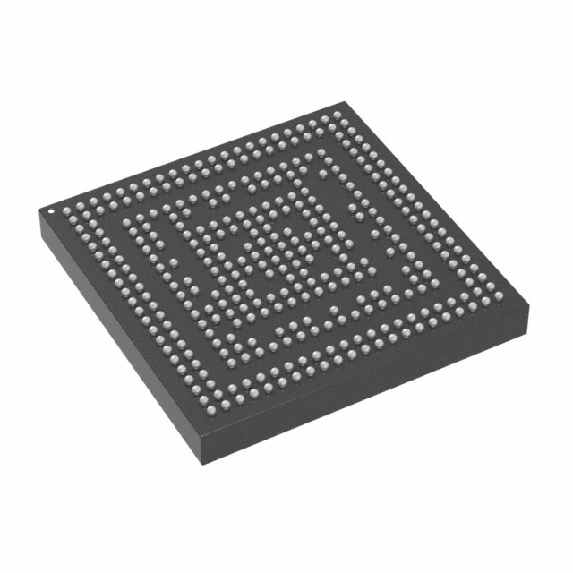
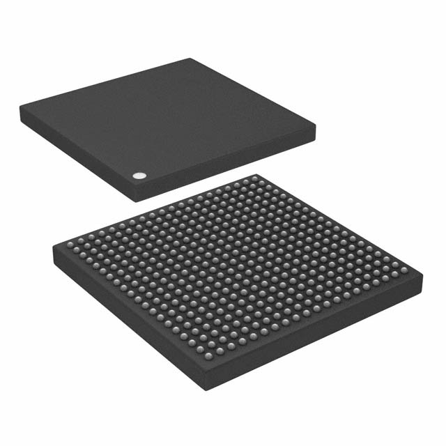
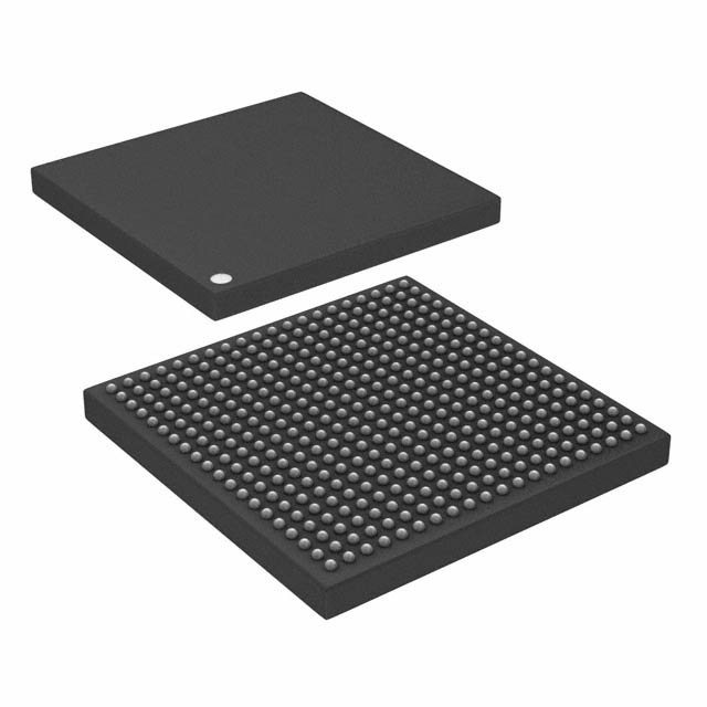
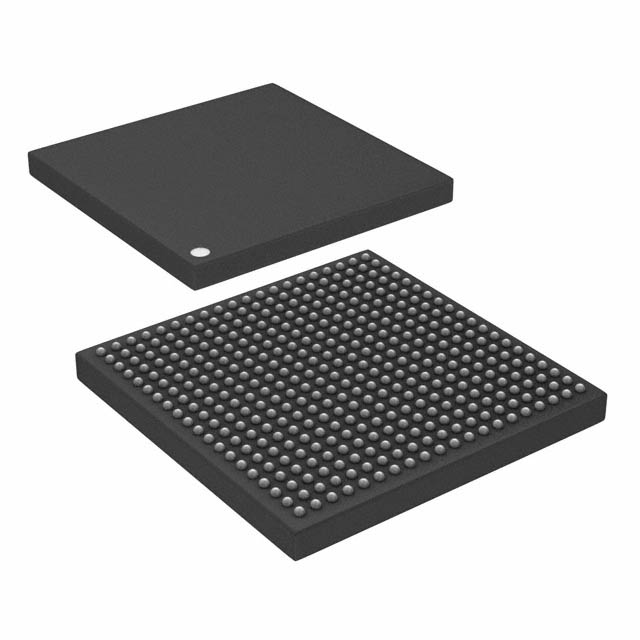
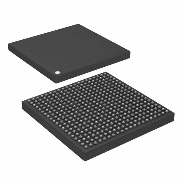
ARM926EJ-S Microprocessor IC i.MX25 1 Core, 32-Bit 400MHz 400-LFBGA (17x17) |
|---|---|
| Quantity | 1,049 Available (as of October 8, 2026) |

| Product Category | Microprocessors |
|---|---|
| Part Series | i.MX 257 |
| Manufacturer | NXP USA Inc. |
| Manufacturing Status | Active |
| Manufacturer Standard Lead Time | 16 Weeks |
| Datasheet |
Specifications & Environmental
| Core Processor | ARM926EJ-S | Device Package | 400-LFBGA (17x17) | Display & Interface Controllers | Keypad, LCD, Touchscreen | ||
|---|---|---|---|---|---|---|---|
| ECCN | 5A992C | Ethernet | 10/100Mbps (1) | Graphics Acceleration | No | ||
| HTS Code | 8542.31.0001 | Moisture Sensitivity Level | 3 (168 Hours) | Mounting Method | Surface Mount | ||
| Mounting Type | Surface Mount | Number of Cores/Bus Width | 1 Core, 32-Bit | Operating Temperature | -20°C ~ 70°C (TA) | ||
| Package / Case | 400-LFBGA | RAM Controllers | LPDDR, DDR, DDR2 | REACH Compliance | REACH Unaffected | ||
| RoHS Compliance | ROHS3 Compliant | Speed | 400MHz | Supplier Device Package | 400-LFBGA (17×17) | ||
| USB | USB 2.0 + PHY (2) | Voltage – I/O | 2.0V, 2.5V, 2.7V, 3.0V, 3.3V |
Overview of MCIMX257DJM4AR2 – IC MPU I.MX25 400MHZ 400LFBGA
The MCIMX257DJM4AR2 is an NXP Semiconductors i.MX25 series applications processor featuring a single ARM926EJ‑S core running at up to 400 MHz. Designed for embedded and consumer applications, the device combines processing performance with power management and integrated peripherals to support compact, connected systems.
Typical markets include industrial and general embedded systems where support for external DDR/DDR2/LPDDR memory, on‑chip Ethernet and USB connectivity, and display/input interfaces are required. The i.MX25 architecture targets use cases that need efficient multimedia handling, connectivity, and low system power.
Key Features
- Core — ARM926EJ‑S 32‑bit processor core operating up to 400 MHz, providing a balance of performance and low power for embedded applications.
- Memory Interfaces — Integrated memory controllers supporting LPDDR, DDR and DDR2, with documented support in the datasheet for up to 133 MHz DDR2 operation.
- Connectivity — Integrated 10/100 Mbps Ethernet MAC and two USB 2.0 ports with on‑chip PHYs to simplify system-level connectivity.
- Display & Input — On‑chip controllers for LCD, keypad and touchscreen interfaces to support human‑machine interfaces and graphical remote controls.
- Additional Interfaces — CAN interface and other peripheral connectivity options for integration into control and gateway devices.
- Power Management — Advanced on‑chip power management features documented in the datasheet to optimize system power in active and low‑power modes.
- Package & Mounting — 400‑LFBGA package (17 × 17 mm, 0.8 mm pitch) in a surface‑mount form factor suitable for compact, high‑density PCB designs.
- Operating Range & Compliance — Consumer qualification with operating temperature range of −20 °C to 70 °C and RoHS compliance.
Typical Applications
- Graphical Remote Controls — Drives LCD and touchscreen interfaces while providing USB and Ethernet connectivity for firmware updates and peripheral integration.
- Human Machine Interface (HMI) — Supports keypad and display controllers for control panels and operator interfaces in residential and commercial equipment.
- Residential Gateways & Smart Metering — Integrates networking and peripheral interfaces to serve as a communications and control processor in gateway or metering devices.
- Handheld Scanners & Point‑of‑Sale Terminals — Combines processing, memory interface flexibility, and USB connectivity for portable scanning and payment terminals.
- Medical Monitoring Devices — Suitable for patient‑monitoring applications requiring embedded processing, display interfaces, and reliable connectivity in consumer‑grade environments.
Unique Advantages
- Highly integrated connectivity: On‑chip 10/100 Ethernet MAC and dual USB 2.0 PHYs reduce external components and simplify board design.
- Flexible memory support: Controllers for LPDDR, DDR and DDR2 enable designers to choose memory technologies that match cost and performance targets.
- Compact package: 400‑LFBGA (17 × 17 mm) package supports high pin count in a compact footprint for space‑constrained designs.
- Power management features: Integrated power management capabilities documented in the datasheet help minimize system power in both active and low‑power states.
- Broad application fit: Documented use cases in consumer and industrial embedded products make the device suitable for a range of HMIs, gateways, and handheld systems.
- RoHS compliant and consumer qualified: Meets regulatory and market expectations for consumer electronics deployments.
Why Choose MCIMX257DJM4AR2?
The MCIMX257DJM4AR2 positions itself as a balanced, integrated processor option for embedded designs that require a proven ARM926EJ‑S core at 400 MHz, flexible memory interfacing, and built‑in connectivity options. Its combination of Ethernet, dual USB PHYs, and display/input controllers reduces system complexity and BOM for compact, connected devices.
Backed by NXP Semiconductors documentation and datasheet support, the i.MX25 family offers a practical platform for designers targeting consumer and general embedded markets who need reliable performance, power management, and peripheral integration.
Request a quote or submit a pricing and availability inquiry to move your design forward with the MCIMX257DJM4AR2.




















Date Founded: 2006
Headquarters: Eindhoven, North Brabant, Netherlands
Employees: 38,000+
Revenue: $10.53 Billion
Certifications and Memberships: ISO9001:2015, IATF16949:2016


