
MCIMX280DVM4C
| Part Description |
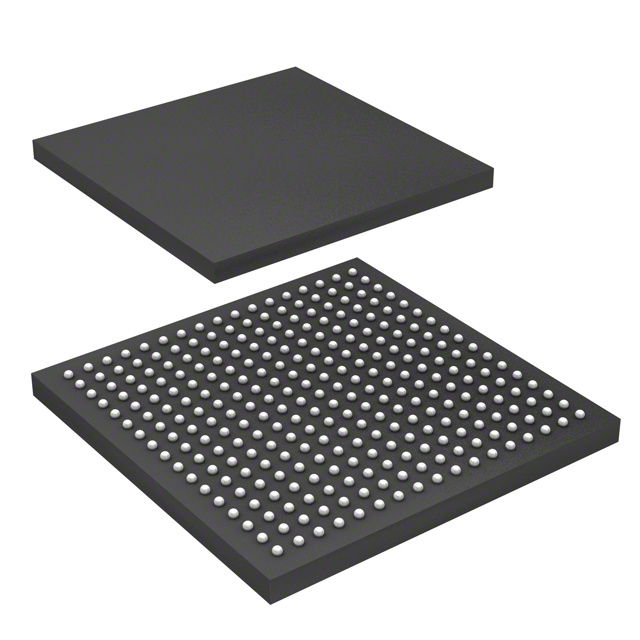
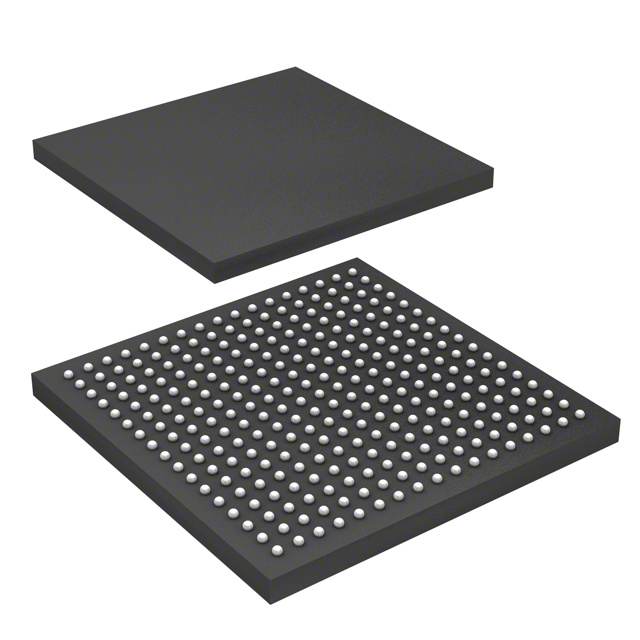
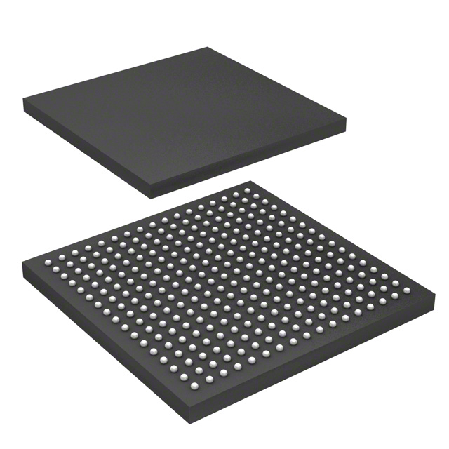
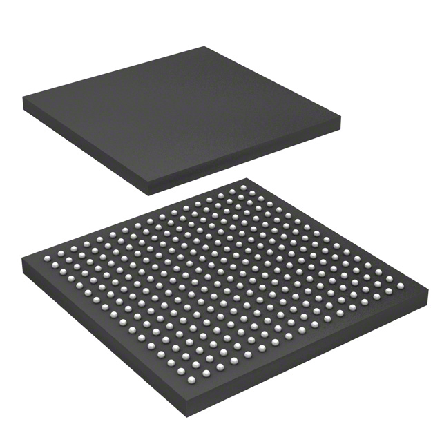
ARM926EJ-S Microprocessor IC i.MX28 1 Core, 32-Bit 454MHz 289-MAPBGA (14x14) |
|---|---|
| Quantity | 55 Available (as of October 7, 2026) |

| Product Category | Microprocessors |
|---|---|
| Part Series | i.MX 280 |
| Manufacturer | NXP USA Inc. |
| Manufacturing Status | Active |
| Manufacturer Standard Lead Time | 20 Weeks |
| Datasheet |
Specifications & Environmental
| Co-Processors/DSP | Data; DCP | Core Processor | ARM926EJ-S | Device Package | 289-MAPBGA (14x14) | ||
|---|---|---|---|---|---|---|---|
| Display & Interface Controllers | Keypad | ECCN | 5A992C | Ethernet | 10/100Mbps (1) | ||
| Graphics Acceleration | No | HTS Code | 8542.31.0001 | Moisture Sensitivity Level | 3 (168 Hours) | ||
| Mounting Method | Surface Mount | Mounting Type | Surface Mount | Number of Cores/Bus Width | 1 Core, 32-Bit | ||
| Operating Temperature | -20°C ~ 70°C (TA) | Package / Case | 289-LFBGA | RAM Controllers | LVDDR, LVDDR2, DDR2 | ||
| REACH Compliance | REACH Unaffected | RoHS Compliance | ROHS3 Compliant | Security Features | Boot Security, Cryptography, Hardware ID | ||
| Speed | 454MHz | Supplier Device Package | 289-MAPBGA (14×14) | USB | USB 2.0 + PHY (2) | ||
| Voltage – I/O | 1.8V, 3.3V |
Overview of MCIMX280DVM4C – IC MPU I.MX28 454MHz 289-MAPBGA
The MCIMX280DVM4C is an NXP Semiconductors i.MX28 applications processor built around a single ARM926EJ-S 32‑bit core running at up to 454 MHz. It is a low-power, highly integrated MPU optimized for embedded consumer and industrial applications that require compact system design and power management integration.
Designed for human‑machine interfaces, industrial control, handheld devices and smart energy products, the device combines processing performance with on-chip system features to simplify board-level design and system power sequencing.
Key Features
- Core ARM926EJ‑S single 32‑bit core running up to 454 MHz, providing deterministic embedded processing for control and HMI tasks.
- On‑chip Memory Includes 128 KB on‑chip SRAM to support small-footprint RTOS designs and reduce the need for external RAM in low‑memory applications.
- Memory Interfaces Controllers for LVDDR, LVDDR2 and DDR2 external memories enable flexible system memory configurations.
- Integrated Power Management On-chip PMU with a triple-output DC‑DC switching converter and multiple linear regulators provides device and I/O power sequencing and supports Li‑Ion battery charging functionality.
- Connectivity Integrated 10/100 Mbps Ethernet interface and two USB 2.0 controllers with PHYs enable wired networking and host/device USB connectivity.
- Security Boot security, cryptographic capabilities and a hardware ID are provided for device identity and secure boot implementations.
- Peripheral Interfaces I2C and keypad display controller support common embedded peripherals and simple user interfaces.
- Package & Mounting 289‑MAPBGA 14 × 14 mm package (289‑LFBGA case), surface mount, suitable for compact board layouts.
- Operating Range & Qualification Consumer‑qualified device with an operating temperature range of −20 °C to 70 °C.
Typical Applications
- Human‑Machine Interface (HMI) Panels — Drives industrial and home HMI panels with integrated power sequencing and interface support for keypads and displays.
- Industrial Control & PLCs — Suitable for factory automation, drive control and I/O modules where deterministic processing and power management are required.
- Handheld Scanners & Printers — Compact MPU with on‑chip SRAM and multiple peripheral interfaces to support portable imaging and printing devices.
- Portable Medical Devices — Supports patient‑monitoring and other portable medical instruments that need reliable processing and power management.
- Smart Energy Meters & Gateways — Provides connectivity and secure boot capabilities for energy metering and gateway applications.
Unique Advantages
- Highly integrated power management: On‑chip PMU with DC‑DC converter and linear regulators reduces external power components and simplifies power sequencing.
- Reduced external memory needs: Built‑in 128 KB SRAM can eliminate external RAM in small RTOS footprints, lowering BOM and board area.
- Flexible memory support: Controllers for LVDDR, LVDDR2 and DDR2 allow designers to choose memory technologies that match performance and cost targets.
- Built‑in connectivity: 10/100 Mbps Ethernet plus two USB 2.0 + PHY ports enable networked and peripheral‑rich designs without additional controllers.
- Security features for product integrity: Boot security, cryptography and hardware ID support secure device identity and authenticated boot flows.
- Compact, production‑ready package: 289‑MAPBGA (14 × 14 mm) surface‑mount package facilitates dense PCB layouts for compact products.
Why Choose MCIMX280DVM4C?
The MCIMX280DVM4C combines an efficient ARM926EJ‑S core with integrated power management, on‑chip SRAM and a broad set of interfaces to deliver a compact, system‑oriented MPU for embedded consumer and industrial designs. Its combination of processing performance, integrated PMU and security features makes it a practical choice for HMI, handheld, medical and smart energy applications where board space and BOM reduction matter.
Backed by NXP Semiconductors' i.MX28 family documentation and package options, this device is suited for customers seeking a stable, well‑documented MPU platform with flexible memory and peripheral support for medium‑complexity embedded products.
If you would like pricing or availability, request a quote or submit an inquiry to receive a formal quote and additional ordering information.























Date Founded: 2006
Headquarters: Eindhoven, North Brabant, Netherlands
Employees: 38,000+
Revenue: $10.53 Billion
Certifications and Memberships: ISO9001:2015, IATF16949:2016


