
MCIMX283DVM4B
| Part Description |
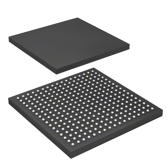
ARM926EJ-S Microprocessor IC i.MX28 1 Core, 32-Bit 454MHz 289-MAPBGA (14x14) |
|---|---|
| Quantity | 1,621 Available (as of October 7, 2026) |
| Product Category | Microprocessors |
|---|---|
| Part Series | i.MX 283 |
| Manufacturer | NXP USA Inc. |
| Manufacturing Status | Active |
| Manufacturer Standard Lead Time | 20 Weeks |
| Datasheet |
Specifications & Environmental
| Co-Processors/DSP | Data; DCP | Core Processor | ARM926EJ-S | Device Package | 289-MAPBGA (14x14) | ||
|---|---|---|---|---|---|---|---|
| Display & Interface Controllers | Keyboard, LCD, Touchscreen | ECCN | 5A992C | Ethernet | 10/100Mbps (1) | ||
| Graphics Acceleration | No | HTS Code | 8542.31.0001 | Moisture Sensitivity Level | 3 (168 Hours) | ||
| Mounting Method | Surface Mount | Mounting Type | Surface Mount | Number of Cores/Bus Width | 1 Core, 32-Bit | ||
| Operating Temperature | -20°C ~ 70°C (TA) | Package / Case | 289-LFBGA | RAM Controllers | LVDDR, LVDDR2, DDR2 | ||
| REACH Compliance | REACH Unaffected | RoHS Compliance | ROHS3 Compliant | Security Features | Boot Security, Cryptography, Hardware ID | ||
| Speed | 454MHz | Supplier Device Package | 289-MAPBGA (14×14) | USB | USB 2.0 + PHY (2) | ||
| Voltage – I/O | 1.8V, 3.3V |
Overview of MCIMX283DVM4B – IC MPU I.MX28 454MHz 289-MAPBGA
The MCIMX283DVM4B is an applications microprocessor from NXP Semiconductors based on the ARM926EJ-S core running at up to 454 MHz. It is a single‑core, 32‑bit processor optimized for embedded industrial and consumer applications that require a balance of performance and power efficiency.
Designed for human‑machine interfaces, portable devices and industrial control, the i.MX28 series integrates power management and on‑chip SRAM while supporting a range of external memories and common peripheral interfaces to simplify system design.
Key Features
- ARM Core The device implements an ARM926EJ‑S core with a single 32‑bit processing core operating up to 454 MHz.
- On‑chip SRAM Includes an additional 128‑Kbyte on‑chip SRAM to reduce or eliminate external RAM in small‑footprint RTOS designs.
- Integrated Power Management On‑chip PMU composed of a triple‑output DC‑DC switching converter and multiple linear regulators to manage power sequencing and battery charging for Li‑Ion cells.
- Memory Support Supports connections to mobile DDR, DDR2 and LV‑DDR2 memories, and external NAND Flash (SLC/MLC) through compatible controllers.
- Connectivity Integrated 10/100 Mbps Ethernet interface (1), and dual USB 2.0 controllers with PHY (2) for device and host connectivity.
- Display & Input Display interface controllers include support for keyboard, LCD and touchscreen interfaces for HMI applications.
- Security Built‑in boot security, cryptography and hardware ID features to support secure boot and device identity.
- DSP & Acceleration Includes Data Co‑Processor (DCP) for data processing and cryptographic acceleration tasks.
- Package & Mounting Available in a 289‑MAPBGA package (289‑LFBGA reference) in a 14 x 14 mm footprint, surface mount.
- Operating Range Qualified for consumer applications with an operating temperature range of −20 °C to 70 °C.
- RoHS Compliance Device is RoHS compliant.
Typical Applications
- HMI Panels Industrial and home human‑machine interfaces, leveraging LCD and touchscreen controllers for responsive displays and input.
- Industrial Control PLCs, drive controllers, factory robotics displays and I/O control panels that benefit from integrated power sequencing and robust connectivity.
- Handheld Devices Scanners, portable printers and handheld terminals that require compact packaging, integrated PMU and on‑chip SRAM for reduced BOM.
- Medical & Portable Monitoring Patient‑monitoring and portable medical devices that use the processor’s low‑power profile and security features for safe operation.
- Smart Energy Smart meters and energy gateways where secure boot, networking and flexible memory support are important.
Unique Advantages
- Highly integrated power management: On‑chip triple output DC‑DC converter and multiple linear regulators simplify power design and enable battery charging support for Li‑Ion systems.
- Reduced external memory needs: The additional 128‑Kbyte on‑chip SRAM helps lower BOM and board area for small RTOS applications.
- Flexible memory interfaces: Controllers for LVDDR, LVDDR2 and DDR2 plus support for NAND Flash provide design flexibility across a range of storage and performance requirements.
- Built‑in security primitives: Boot security, cryptography and hardware ID features support device authentication and secure boot flows.
- Broad connectivity: Integrated Ethernet and dual USB 2.0 with PHY make networked and peripheral‑rich designs straightforward to implement.
- Compact, production‑ready package: 289‑MAPBGA (14 x 14 mm) surface‑mount package suitable for space‑constrained embedded systems.
Why Choose MCIMX283DVM4B?
The MCIMX283DVM4B positions itself as a balanced, low‑power, high‑performance application processor for embedded and consumer products. With an ARM926EJ‑S core at up to 454 MHz, integrated power management, on‑chip SRAM and a broad set of peripheral interfaces, it enables designers to reduce BOM and accelerate time to market for HMI, portable and industrial control applications.
Manufactured by NXP Semiconductors and backed by the i.MX28 family documentation, this part is suitable for designs that require compact packaging, flexible memory options and built‑in security features while targeting consumer operating temperature ranges.
Request a quote or submit an inquiry to obtain pricing, availability and ordering information for the MCIMX283DVM4B.
























Date Founded: 2006
Headquarters: Eindhoven, North Brabant, Netherlands
Employees: 38,000+
Revenue: $10.53 Billion
Certifications and Memberships: ISO9001:2015, IATF16949:2016


