
MCIMX6Y2CVM08ABR
| Part Description |
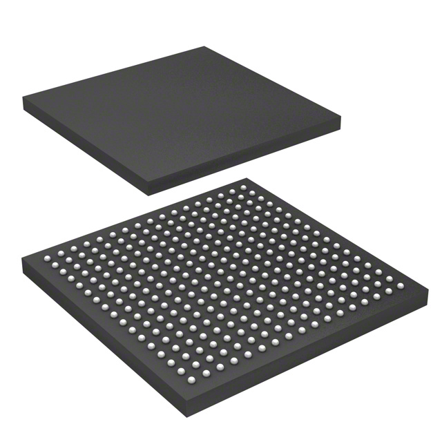
ARM® Cortex®-A7 Microprocessor IC i.MX6 1 Core, 32-Bit 792MHz 289-MAPBGA (14x14) |
|---|---|
| Quantity | 211 Available (as of October 8, 2026) |

| Product Category | Microprocessors |
|---|---|
| Part Series | i.MX 6Y |
| Manufacturer | NXP USA Inc. |
| Manufacturing Status | Active |
| Manufacturer Standard Lead Time | 16 Weeks |
| Datasheet |
Specifications & Environmental
| Co-Processors/DSP | Multimedia; NEON™ MPE | Core Processor | ARM® Cortex®-A7 | Device Package | 289-MAPBGA (14x14) | ||
|---|---|---|---|---|---|---|---|
| Display & Interface Controllers | Electrophoretic, LCD | ECCN | N/A | Ethernet | 10/100Mbps (2) | ||
| Graphics Acceleration | No | HTS Code | N/A | Moisture Sensitivity Level | N/A | ||
| Mounting Method | Surface Mount | Mounting Type | Surface Mount | Number of Cores/Bus Width | 1 Core, 32-Bit | ||
| Operating Temperature | -40°C ~ 105°C (TJ) | Package / Case | 289-LFBGA | RAM Controllers | LPDDR2, DDR3, DDR3L | ||
| REACH Compliance | REACH Unaffected | RoHS Compliance | ROHS3 Compliant | Security Features | A-HAB, ARM TZ, CSU, SJC, SNVS | ||
| Speed | 792MHz | Supplier Device Package | 289-MAPBGA (14×14) | USB | USB 2.0 OTG + PHY (2) | ||
| Voltage – I/O | 1.8V, 2.8V, 3.3V |
Overview of MCIMX6Y2CVM08ABR – 32‑Bit ARM® Cortex®‑A7 MPU, 792 MHz
The MCIMX6Y2CVM08ABR is a single‑core 32‑bit microprocessor based on the ARM® Cortex®‑A7 architecture, running at 792 MHz. Designed for embedded and industrial applications, it combines a compact MAPBGA package, broad peripheral support and on‑chip integration to simplify system design and deployment.
Targeted use cases include connected devices and embedded systems requiring a balanced mix of processing, multimedia offload and industrial‑grade reliability, while maintaining support for multiple memory types and common peripheral interfaces.
Key Features
- Core – ARM® Cortex®‑A7 single core, 32‑bit at 792 MHz, providing deterministic application processing for embedded workloads.
- Multimedia Acceleration – Includes multimedia co‑processors and NEON™ MPE for SIMD acceleration of media and signal processing tasks.
- Memory support – RAM controllers for LPDDR2, DDR3 and DDR3L; family datasheet also describes support for raw/managed NAND, NOR flash, eMMC and Quad SPI memory interfaces for flexible storage options.
- Display and UI – Display interface controllers for electrophoretic (E‑ink) and LCD panels, suitable for embedded user interfaces and low‑power displays.
- Connectivity – Dual 10/100 Mbps Ethernet ports, two USB 2.0 OTG ports with PHY, and CANbus for industrial and networked I/O needs.
- Security – Hardware security features including A‑HAB, ARM TrustZone (ARM TZ), CSU, SJC and SNVS to support secure boot and runtime security domains.
- Power and integration – Series documentation highlights an integrated power management module and on‑chip regulators to reduce external power sequencing complexity.
- Package & mounting – 289‑MAPBGA supplier device package (14 × 14 mm), surface‑mount for compact board integration.
- Industrial qualification & temperature – Industrial qualification with an operating temperature range of −40 °C to 105 °C for harsh environments.
- Compliance – RoHS compliant.
- Graphics acceleration – No dedicated graphics acceleration; suitable when pixel rendering or advanced GPU features are not required.
Typical Applications
- Industrial controllers – Deterministic application processing and CANbus plus dual Ethernet support make this MPU suitable for embedded control and automation nodes.
- Connected sensors and gateways – Multiple USB, Ethernet and CAN interfaces allow protocol bridging and local processing in IoT gateway and sensor aggregation roles.
- Low‑power displays and HMI – Electrophoretic and LCD display controllers enable battery‑friendly interfaces and simple operator displays.
- Appliances and consumer embedded devices – Integrated memory interfaces and secure boot features are useful for consumer products requiring moderate application processing and content protection.
Unique Advantages
- Balanced processing and efficiency – A Cortex‑A7 core at 792 MHz provides a practical tradeoff between compute capability and power for embedded workloads.
- Comprehensive memory options – Support for LPDDR2, DDR3, DDR3L and a range of flash interfaces simplifies BOM choices and enables scalable memory configurations.
- Industrial readiness – Industrial qualification and a −40 °C to 105 °C operating range support deployment in demanding environments.
- Built‑in security primitives – A‑HAB, ARM TrustZone and related security modules help implement secure boot and protect sensitive operations.
- Connectivity breadth – Dual Ethernet, USB OTG with PHY and CANbus deliver multiple paths for networking and peripheral interfacing without extensive external logic.
- Compact, surface‑mount package – The 289‑MAPBGA (14 × 14 mm) footprint enables high‑density board designs while maintaining robust pinout capability.
Why Choose MCIMX6Y2CVM08ABR?
MCIMX6Y2CVM08ABR is positioned for embedded and industrial designs that require a compact, integrated processor with a secure foundation and versatile I/O. Its ARM® Cortex®‑A7 core, combined with multiple memory interfaces, dual Ethernet and USB OTG, delivers practical processing and connectivity for a wide range of applications.
Backed by NXP Semiconductors’ platform documentation and product family features—such as integrated power management and extensive peripheral support—this MPU offers designers a clear path to scalable, robust products that meet industrial operating requirements.
Request a quote or submit a pricing inquiry to evaluate MCIMX6Y2CVM08ABR for your next embedded design.





















Date Founded: 2006
Headquarters: Eindhoven, North Brabant, Netherlands
Employees: 38,000+
Revenue: $10.53 Billion
Certifications and Memberships: ISO9001:2015, IATF16949:2016


